
Datasheet


74LVC2G07 All information provided in this document is subject to legal disclaimers. © NXP B.V. 2012. All rights reserved.
Product data sheet Rev. 7 — 4 July 2012 3 of 18
NXP Semiconductors
74LVC2G07
Buffers with open-drain outputs
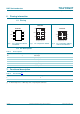
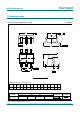
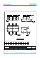
6. Pinning information
6.1 Pinning
6.2 Pin description
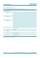
7. Functional description
[1] H = HIGH voltage level; L = LOW voltage level; Z = high-impedance OFF-state.
Fig 4. Pin configuration SOT363
and SOT457
Fig 5. Pin configuration SOT886 Fig 6. Pin configuration SOT891,
SOT1115 and SOT1202
74LVC2G07
1A 1Y
GND
2A 2Y
001aab670
1
2
3
6
V
CC
5
4
74LVC2G07
GND
001aab671
1A
2A
V
CC
1Y
2Y
Transparent top view
2
3
1
5
4
6
74LVC2G07
GND
001aag423
1A
2A
V
CC
1Y
2Y
Transparent top view
2
3
1
5
4
6
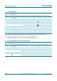
Table 3. Pin description
Symbol Pin Description
1A 1 data input
GND 2 ground (0 V)
2A 3 data input
2Y 4 data output
V
CC
5 supply voltage
1Y 6 data output
Table 4. Function table
[1]
Input nA Output nY
LL
HZ