
Datasheet


74LVC2G07 All information provided in this document is subject to legal disclaimers. © NXP B.V. 2012. All rights reserved.
Product data sheet Rev. 7 — 4 July 2012 8 of 18
NXP Semiconductors
74LVC2G07
Buffers with open-drain outputs
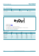
Table 9. Measurement points
Supply voltage Input Output
V
CC
V
M
V
M
V
X
1.65 V to 1.95 V 0.5 V
CC
0.5 V
CC
V
OL
+ 0.15 V
2.3 V to 2.7 V 0.5 V
CC
0.5 V
CC
V
OL
+ 0.15 V
2.7 V 1.5 V 1.5 V V
OL
+ 0.3 V
3.0 V to 3.6 V 1.5 V 1.5 V V
OL
+ 0.3 V
4.5 V to 5.5 V 0.5 V
CC
0.5 V
CC
V
OL
+ 0.3 V
Test data is given in Table 10.
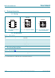
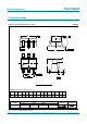
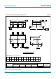
Definitions for test circuit:
R
L
= Load resistance.
C
L
= Load capacitance including jig and probe capacitance.
R
T
= Termination resistance should be equal to the output impedance Z
o
of the pulse generator.
V
EXT
= External voltage for measuring switching times.
Fig 8. Test circuit for measuring switching times
V
EXT
V
CC
V
I
V
O
mna616
DUT
C
L
R
T
R
L
R
L
G
Table 10. Test data
Supply voltage Input Load V
EXT
V
CC
V
I
t
r
, t
f
C
L
R
L
t
PZL
, t
PLZ
1.65 V to 1.95 V V
CC
2.0 ns 30 pF 1 k 2 V
CC
2.3 V to 2.7 V V
CC
2.0 ns 30 pF 500 2 V
CC
2.7 V 2.7 V 2.5 ns 50 pF 500 6 V
3.0 V to 3.6 V 2.7 V 2.5 ns 50 pF 500 6 V
4.5 V to 5.5 V V
CC
2.5 ns 50 pF 500 2 V
CC