
Datasheet

1. General description
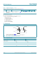
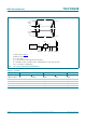
The 74LVC2G08 provides a 2-input AND gate function.
Inputs can be driven from either 3.3 V or 5 V devices. This feature allows the use of the
74LVC2G08 as a translator in a mixed 3.3 V and 5 V environment.
This device is fully specified for partial power-down applications using I
OFF
. The I
OFF
circuitry disables the output, preventing a damaging backflow current through the device
when it is powered down.
2. Features and benefits
Wide supply voltage range from 1.65 V to 5.5 V
5 V tolerant outputs for interfacing with 5 V logic
High noise immunity
24 mA output drive (V
CC
=3.0V)
CMOS low power consumption
Complies with JEDEC standard:
JESD8-7 (1.65 V to 1.95 V)
JESD8-5 (2.3 V to 2.7 V)
JESD8-B/JESD36 (2.7 V to 3.6 V)
Latch-up performance exceeds 250 mA
Direct interface with TTL levels
Inputs accept voltages up to 5 V
ESD protection:
HBM JESD22-A114F exceeds 2000 V
MM JESD22-A115-A exceeds 200 V
Multiple package options
Specified from 40 Cto +85C and 40 Cto+125C
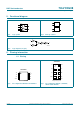
74LVC2G08
Dual 2-input AND gate
Rev. 12 — 2 April 2013 Product data sheet