
Datasheet

74LVC2G08 All information provided in this document is subject to legal disclaimers. © NXP B.V. 2013. All rights reserved.
Product data sheet Rev. 12 — 2 April 2013 3 of 21
NXP Semiconductors
74LVC2G08
Dual 2-input AND gate
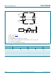
5. Functional diagram
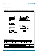
6. Pinning information
6.1 Pinning
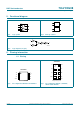
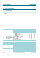
Fig 1. Logic symbol Fig 2. IEC logic symbol
001aah788
1A
1B
1Y
2A
2B
2Y
001aah789
&
&
Fig 3. Logic diagram (one gate)
mna221
A
B
Y
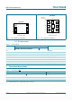
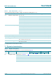
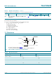
Fig 4. Pin configuration SOT505-2 and SOT765-1 Fig 5. Pin configuration SOT833-1, SOT1089,
SOT1116 and SOT1203
74LVC2G08
1A V
CC
1B 1Y
2Y 2B
GND 2A
001aae981
1
2
3
4
6
5
8
7
74LVC2G08
2B
1Y
V
CC
2A
2Y
1B
1A
GND
001aae982
36
27
18
45
Transparent top view