
Datasheet

74LVC2G08 All information provided in this document is subject to legal disclaimers. © NXP B.V. 2013. All rights reserved.
Product data sheet Rev. 12 — 2 April 2013 8 of 21
NXP Semiconductors
74LVC2G08
Dual 2-input AND gate
[1] Typical values are measured at nominal V
CC
and at T
amb
= 25 C.
[2] t
pd
is the same as t
PLH
and t
PHL
[3] C
PD
is used to determine the dynamic power dissipation (P
D
in W).
P
D
= C
PD
V
CC
2
f
i
N + (C
L
V
CC
2
f
o
) where:
f
i
= input frequency in MHz;
f
o
= output frequency in MHz;
C
L
= output load capacitance in pF;
V
CC
= supply voltage in V;
N = number of inputs switching;
(C
L
V
CC
2
f
o
) = sum of outputs.
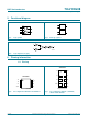
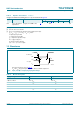
12. Waveforms
C
PD
power dissipation
capacitance
per gate; V
I
= GND to V
CC
[3]
- 14.4 - - - pF
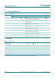
Table 8. Dynamic characteristics
…continued
Voltages are referenced to GND (ground = 0 V); for test circuit see Figure 9.
Symbol Parameter Conditions 40 C to +85 C 40 C to +125 C Unit
Min Typ
[1]
Max Min Max
Measurement points are given in Table 9.
V
OL
and V
OH
are typical output voltage levels that occur with the output load.
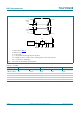
Fig 8. Input (nA, nB) to output (nY) propagation delays
mna224
nA, nB input
nY output
t
PLH
t
PHL
GND
V
I
V
M
V
M
V
OH
V
OL
Table 9. Measurement points
Supply voltage Input Output
V
CC
V
M
V
M
1.65 V to 1.95 V 0.5 V
CC
0.5 V
CC
2.3 V to 2.7 V 0.5 V
CC
0.5 V
CC
2.7 V 1.5 V 1.5 V
3.0 V to 3.6 V 1.5 V 1.5 V
4.5 V to 5.5 V 0.5 V
CC
0.5 V
CC