
Datasheet

74LVC2G126 All information provided in this document is subject to legal disclaimers. © NXP B.V. 2013. All rights reserved.
Product data sheet Rev. 12 — 8 April 2013 2 of 22
NXP Semiconductors
74LVC2G126
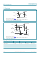
Dual bus buffer/line driver; 3-state
3. Ordering information
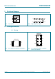
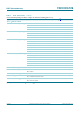
4. Marking
[1] The pin 1 indicator is located on the lower left corner of the device, below the marking code.
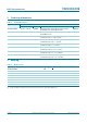
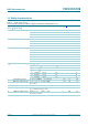
Table 1. Ordering information
Type number Package
Temperature range Name Description Version
74LVC2G126DP 40 Cto+125C TSSOP8 plastic thin shrink small outline package; 8 leads;
body width 3 mm; lead length 0.5 mm
SOT505-2
74LVC2G126DC 40 Cto+125C VSSOP8 plastic very thin shrink small outline package; 8 leads;
body width 2.3 mm
SOT765-1
74LVC2G126GT 40 Cto+125C XSON8 plastic extremely thin small outline package; no leads;
8 terminals; body 1 1.95 0.5 mm
SOT833-1
74LVC2G126GF 40 C to +125 C XSON8 extremely thin small outline package; no leads;
8 terminals; body 1.35 1 0.5 mm
SOT1089
74LVC2G126GD 40 Cto+125C XSON8 plastic extremely thin small outline package; no leads;
8 terminals; body 3 2 0.5 mm
SOT996-2
74LVC2G126GM 40 C to +125 C XQFN8 plastic, extremely thin quad flat package; no leads;
8 terminals; body 1.6 1.6 0.5 mm
SOT902-2
74LVC2G126GN 40 C to +125 C XSON8 extremely thin small outline package; no leads;
8 terminals; body 1.2 1.0 0.35 mm
SOT1116
74LVC2G126GS 40 C to +125 C XSON8 extremely thin small outline package; no leads;
8 terminals; body 1.35 1.0 0.35 mm
SOT1203
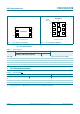
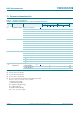
Table 2. Marking codes
Type number Marking code
[1]
74LVC2G126DP V26
74LVC2G126DC V26
74LVC2G126GT V26
74LVC2G126GF VN
74LVC2G126GD V26
74LVC2G126GM V26
74LVC2G126GN VN
74LVC2G126GS VN