
Datasheet

74LVC2G126 All information provided in this document is subject to legal disclaimers. © NXP B.V. 2013. All rights reserved.
Product data sheet Rev. 12 — 8 April 2013 3 of 22
NXP Semiconductors
74LVC2G126
Dual bus buffer/line driver; 3-state
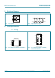
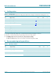
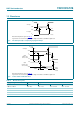
5. Functional diagram
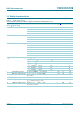
6. Pinning information
6.1 Pinning
Fig 1. Logic symbol Fig 2. Logic diagram (one gate)
001aah787
2A
1A
2OE
1OE
1Y
2Y
mna234
nOE
nA
nY
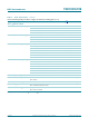
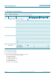
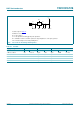
Fig 3. Pin configuration SOT505-2 and SOT765-1 Fig 4. Pin configuration SOT833-1, SOT1089,
SOT1116 and SOT1203
74LVC2G126
1OE V
CC
1A 2OE
2Y 1Y
GND 2A
001aab740
1
2
3
4
6
5
8
7
74LVC2G126
1Y
2OE
V
CC
2A
2Y
1A
1OE
GND
001aab741
36
27
18
45
Transparent top view