
Datasheet

74LVC2G126 All information provided in this document is subject to legal disclaimers. © NXP B.V. 2013. All rights reserved.
Product data sheet Rev. 12 — 8 April 2013 4 of 22
NXP Semiconductors
74LVC2G126
Dual bus buffer/line driver; 3-state
6.2 Pin description
7. Functional description
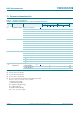
[1] H = HIGH voltage level; L = LOW voltage level; X = don’t care; Z = high-impedance OFF-state.
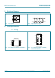
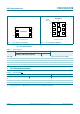
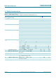
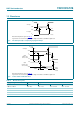
Fig 5. Pin configuration SOT996-2 Fig 6. Pin configuration SOT902-2
001aah949
74LVC2G126
Transparent top view
8
7
6
5
1
2
3
4
1OE
1A
2Y
GND
V
CC
2OE
1Y
2A
001aaf056
1A1Y
1OE
V
CC
2Y
2OE
GND
2A
Transparent top view
3
6
4
1
5
8
7
2
terminal 1
index area
74LVC2G126
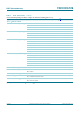
Table 3. Pin description
Symbol Pin Description
SOT505-2, SOT765-1, SOT833-1, SOT1089,
SOT996-2, SOT1116 and SOT1203
SOT902-2
1OE, 2OE 1, 7 7, 1 output enable input (active HIGH)
1A, 2A 2, 5 6, 3 data input
1Y, 2Y 6, 3 2, 5 data output
GND 4 4 ground (0 V)
V
CC
8 8 supply voltage
Table 4. Function table
[1]
Input Output
nOE nA nY
HL L
HHH
LXZ