
Datasheet

74LVC2G126 All information provided in this document is subject to legal disclaimers. © NXP B.V. 2013. All rights reserved.
Product data sheet Rev. 12 — 8 April 2013 8 of 22
NXP Semiconductors
74LVC2G126
Dual bus buffer/line driver; 3-state
11. Dynamic characteristics
[1] Typical values are measured at T
amb
=25C and V
CC
= 1.8 V, 2.5 V, 2.7 V, 3.3 V and 5.0 V respectively.
[2] t
pd
is the same as t
PLH
and t
PHL
[3] t
en
is the same as t
PZH
and t
PZL
[4] t
dis
is the same as t
PLZ
and t
PHZ
[5] C
PD
is used to determine the dynamic power dissipation (P
D
in W).
P
D
=C
PD
V
CC
2
f
i
N+(C
L
V
CC
2
f
o
) where:
f
i
= input frequency in MHz;
f
o
= output frequency in MHz;
C
L
= output load capacitance in pF;
V
CC
= supply voltage in V;
N = number of inputs switching;
(C
L
V
CC
2
f
o
) = sum of outputs.
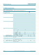
Table 8. Dynamic characteristics
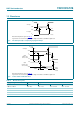
Voltages are referenced to GND (ground = 0 V); for test circuit see Figure 9.
Symbol Parameter Conditions 40 C to +85 C 40 C to +125 C Unit
Min Typ
[1]
Max Min Max
t
pd
propagation delay nA to nY; see Figure 7
[2]
V
CC
= 1.65 V to 1.95 V 1.0 3.9 9.8 1.0 12.3 ns
V
CC
= 2.3 V to 2.7 V 0.5 2.6 4.9 0.5 6.3 ns
V
CC
= 2.7 V 1.0 2.8 4.7 1.0 5.9 ns
V
CC
= 3.0 V to 3.6 V 0.5 2.4 4.3 0.5 5.4 ns
V
CC
= 4.5 V to 5.5 V 0.5 1.9 3.2 0.5 4.0 ns
t
en
enable time nOE to nY; see Figure 8
[3]
V
CC
= 1.65 V to 1.95 V 1.0 4.1 10.0 1.0 12.5 ns
V
CC
= 2.3 V to 2.7 V 1.0 2.6 5.0 1.0 6.3 ns
V
CC
= 2.7 V 1.0 2.8 4.7 1.0 5.9 ns
V
CC
= 3.0 V to 3.6 V 1.0 2.4 4.1 1.0 5.1 ns
V
CC
= 4.5 V to 5.5 V 0.5 1.8 3.1 0.5 3.9 ns
t
dis
disable time nOE to nY; see Figure 8
[4]
V
CC
= 1.65 V to 1.95 V 1.0 3.3 12.6 1.0 15.4 ns
V
CC
= 2.3 V to 2.7 V 0.5 1.9 5.7 0.5 7.5 ns
V
CC
= 2.7 V 1.5 3.0 4.8 1.5 6.2 ns
V
CC
= 3.0 V to 3.6 V 1.0 2.5 4.4 1.0 5.7 ns
V
CC
= 4.5 V to 5.5 V 0.5 1.8 3.3 0.5 4.4 ns
C
PD
power dissipation
capacitance
per buffer; V
I
= GND to V
CC
[5]
output enabled - 17 - - - pF
output disabled - 5 - - - pF