
Datasheet


74LVC2G32_6 © NXP B.V. 2008. All rights reserved.
Product data sheet Rev. 06 — 27 February 2008 4 of 15
NXP Semiconductors
74LVC2G32
Dual 2-input OR gate
7. Functional description
[1] H = HIGH voltage level; L = LOW voltage level.
8. Limiting values
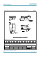
[1] The input and output voltage ratings may be exceeded if the input and output current ratings are observed.
[2] When V
CC
= 0 V (Power-down mode), the output voltage can be 5.5 V in normal condition.
[3] For TSSOP8 package: above 55 °C the value of P
tot
derates linearly with 2.5 mW/K.
For VSSOP8 package: above 110 °C the value of P
tot
derates linearly with 8 mW/K.
For XSON8 and XQFN8U packages: above 45 °C the value of P
tot
derates linearly with 2.4 mW/K.
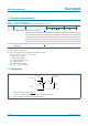
Table 4. Function table
[1]
Input Output
nA nB nY
LLL
LHH
HL H
HHH
Table 5. Limiting values
In accordance with the Absolute Maximum Rating System (IEC 60134). Voltages are referenced to GND (ground = 0 V).
Symbol Parameter Conditions Min Max Unit
V
CC
supply voltage −0.5 +6.5 V
V
I
input voltage
[1]
−0.5 +6.5 V
V
O
output voltage Active mode
[1]
−0.5 V
CC
+ 0.5 V
Power-down mode
[2]
−0.5 +6.5 V
I
IK
input clamping current V
I
<0V −50 - mA
I
OK
output clamping current V
O
< 0 V or V
O
>V
CC
- ±50 mA
I
O
output current V
O
=0VtoV
CC
- ±50 mA
I
CC
supply current - 100 mA
I
GND
ground current −100 - mA
T
stg
storage temperature −65 +150 °C
P
tot
total power dissipation T
amb
= −40 °C to +125 °C
[3]
- 300 mW