
Datasheet


74LVC2G74 All information provided in this document is subject to legal disclaimers. © NXP B.V. 2013. All rights reserved.
Product data sheet Rev. 10 — 2 April 2013 11 of 25
NXP Semiconductors
74LVC2G74
Single D-type flip-flop with set and reset; positive edge trigger
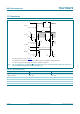
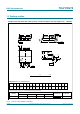
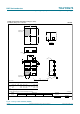
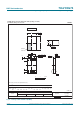
12. Waveforms
Measurement points are given in Table 10.
The shaded areas indicate when the input is permitted to change for predictable output performance.
V
OL
and V
OH
are typical output voltage levels that occur with the output load.
Fig 8. The clock input (CP) to output (Q, Q) propagation delays, the clock pulse width, the D to CP set-up, the
CP to D hold times and the CP maximum frequency
mnb141
t
h
t
su
t
h
t
PHL
t
PHL
t
PLH
t
PLH
t
su
1/f
max
t
W
V
M
V
M
V
M
V
I
GND
V
M
V
I
GND
CP input
D input
V
OH
V
OL
Q output
V
OH
V
OL
Q output
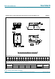
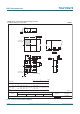
Table 10. Measurement points
Supply voltage Input Output
V
CC
V
M
V
M
1.65 V to 1.95 V 0.5 V
CC
0.5 V
CC
2.3 V to 2.7 V 0.5 V
CC
0.5 V
CC
2.7V 1.5V 1.5V
3.0V to 3.6V 1.5V 1.5V
4.5 V to 5.5 V 0.5 V
CC
0.5 V
CC