
Datasheet


74LVC2G74 All information provided in this document is subject to legal disclaimers. © NXP B.V. 2013. All rights reserved.
Product data sheet Rev. 10 — 2 April 2013 12 of 25
NXP Semiconductors
74LVC2G74
Single D-type flip-flop with set and reset; positive edge trigger
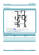
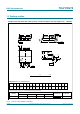
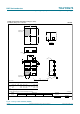
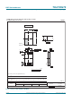
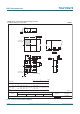
Measurement points are given in Table 10.
V
OL
and V
OH
are typical output voltage levels that occur with the output load.
Fig 9. The set (SD) and reset (RD) input to output (Q, Q) propagation delays, the set and reset pulse widths and
the R
D to CP recovery time
mnb142
t
rec
t
PHL
t
PHL
t
W
t
PLH
t
PLH
V
M
V
M
V
M
t
W
V
M
V
M
V
I
GND
V
I
GND
SD input
V
I
GND
RD input
CP input
V
OH
V
OL
Q output
V
OH
V
OL
Q
output
t
rec