
Datasheet

74LVC541A All information provided in this document is subject to legal disclaimers. © NXP B.V. 2011. All rights reserved.
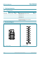
Product data sheet Rev. 4 — 25 November 2011 3 of 17
NXP Semiconductors
74LVC541A
Octal buffer/line driver with 5 V tolerant inputs/outputs; 3-state
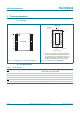
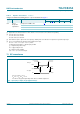
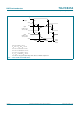
5. Pinning information
5.1 Pinning
5.2 Pin description
(1) This is not a supply pin. The substrate is attached to
this pad using conductive die attach material. There
is no electrical or mechanical requirement to solder
this pad. However, if it is soldered, the solder land
should remain floating or be connected to GND.
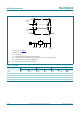
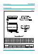
Fig 3. Pin configuration for SO20 and (T)SSOP20 Fig 4. Pin configuration for DHVQFN20
74LVC541A
OE1 V
CC
A0 OE2
A1 Y0
A2 Y1
A3 Y2
A4 Y3
A5 Y4
A6 Y5
A7 Y6
GND Y7
001aad115
1
2
3
4
5
6
7
8
9
10
12
11
14
13
16
15
18
17
20
19
001aad116
74LVC541A
Transparent top view
GND
(1)
GND
Y7
OE1
V
CC
9 12
8 13
7 14
6 15
5 16
4 17
3 18
2 19
10
11
1
20
terminal 1
index area
A0
A1
A2
A3
A4
A5
A6
A7
OE2
Y0
Y1
Y2
Y3
Y4
Y5
Y6
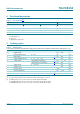
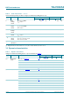
Table 2. Pin description
Symbol Pin Description
OE
1 1 output enable input (active LOW)
A[0:7] 2, 3, 4, 5, 6, 7, 8, 9 data input
GND 10 ground (0 V)
Y[0:7] 18, 17, 16, 15, 14, 13, 12, 11 bus output
OE
2 19 output enable input (active LOW)
V
CC
20 supply voltage