
Datasheet

74LVC541A All information provided in this document is subject to legal disclaimers. © NXP B.V. 2011. All rights reserved.
Product data sheet Rev. 4 — 25 November 2011 4 of 17
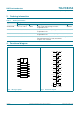
NXP Semiconductors
74LVC541A
Octal buffer/line driver with 5 V tolerant inputs/outputs; 3-state
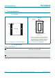
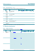
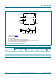
6. Functional description
[1] H = HIGH voltage level
L = LOW voltage level
X = don’t care
Z = high-impedance OFF-state
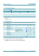
7. Limiting values
[1] The minimum input voltage ratings may be exceeded if the input current ratings are observed.
[2] The output voltage ratings may be exceeded if the output current ratings are observed.
[3] For SO20 packages: above 70 C the value of P
tot
derates linearly with 8 mW/K.
For (T)SSOP20 packages: above 60 C the value of P
tot
derates linearly with 5.5 mW/K.
For DHVQFN20 packages: above 60 C the value of P
tot
derates linearly with 4.5 mW/K.
Table 3. Functional table
[1]
Input Output
OE1 OE2 An Yn
LLLL
LLHH
XHXZ
HXXZ
Table 4. Limiting values
In accordance with the Absolute Maximum Rating System (IEC 60134). Voltages are referenced to GND (ground = 0 V).
Symbol Parameter Conditions Min Max Unit
V
CC
supply voltage 0.5 +6.5 V
I
IK
input clamping current V
I
< 0 V 50 - mA
V
I
input voltage
[1]
0.5 +5.5 V
I
OK
output clamping current V
O
> V
CC
or V
O
< 0 V - 50 mA
V
O
output voltage output HIGH or LOW state
[2]
0.5 V
CC
+ 0.5 V
output 3-state or power-down
[2]
0.5 +6.5 V
I
O
output current V
O
= 0 V to V
CC
- 50 mA
I
CC
supply current - 100 mA
I
GND
ground current 100 - mA
T
stg
storage temperature 60 +150 C
P
tot
total power dissipation T
amb
= 40 C to +125 C
[3]
-500 mW