
Datasheet

74LVC541A All information provided in this document is subject to legal disclaimers. © NXP B.V. 2011. All rights reserved.
Product data sheet Rev. 4 — 25 November 2011 6 of 17
NXP Semiconductors
74LVC541A
Octal buffer/line driver with 5 V tolerant inputs/outputs; 3-state
[1] All typical values are measured at V
CC
= 3.3 V (unless stated otherwise) and T
amb
=25C.
10. Dynamic characteristics
I
I
input
leakage
current
V
I
= 5.5 V or GND;
V
CC
=3.6V
- 0.1 5-20 A
I
OZ
OFF-state
output
current
V
I
=V
IH
or V
IL
;
V
O
=5.5VorGND;
V
CC
=3.6V
- 0.1 5-20 A
I
OFF
power-off
leakage
current
V
I
or V
O
=5.5V; V
CC
= 0.0 V - 0.1 10 - 20 A
I
CC
supply
current
V
I
=V
CC
or GND; I
O
=0A;
V
CC
=3.6V
-0.110 - 40A
I
CC
additional
supply
current
per input pin;
V
I
=V
CC
0.6 V; I
O
=0A;
V
CC
= 2.7 V to 3.6 V
- 5 500 - 5000 A
C
I
input
capacitance
-5.0- - -pF
Table 6. Static characteristics …continued
At recommended operating conditions. Voltages are referenced to GND (ground = 0 V).
Symbol Parameter Conditions 40 C to +85 C 40 C to +125 C Unit
Min Typ
[1]
Max Min Max
Table 7. Dynamic characteristics
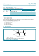
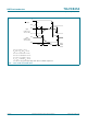
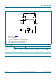
Voltages are referenced to GND (ground = 0 V). For test circuit see Figure 7.
Symbol Parameter Conditions 40 C to +85 C 40 C to +125 C Unit
Min Typ
[1]
Max Min Max
t
pd
propagation
delay
An to Yn; see Figure 5
[2]
V
CC
= 1.2 V - 14.0 - - - ns
V
CC
= 1.65 V to 1.95 V 1.5 6.5 13.8 1.5 16.0 ns
V
CC
= 2.3 V to 2.7 V 1.0 3.5 6.8 1.0 7.9 ns
V
CC
= 2.7 V 1.5 3.5 5.6 1.5 7.0 ns
V
CC
= 3.0 V to 3.6 V 1.0 2.9 5.1 1.0 6.5 ns
t
en
enable time OEn to Yn; see Figure 6
[2]
V
CC
= 1.2 V - 20.0 - - - ns
V
CC
= 1.65 V to 1.95 V 1.8 7.7 16.0 1.8 18.5 ns
V
CC
= 2.3 V to 2.7 V 1.5 4.3 8.8 1.5 10.2 ns
V
CC
= 2.7 V 1.5 4.4 7.5 1.5 9.5 ns
V
CC
= 3.0 V to 3.6 V 1.0 3.5 7.0 1.0 9.0 ns
t
dis
disable time OEn to Yn; see Figure 6
[2]
V
CC
=1.2V - 11.0 - - - ns
V
CC
= 1.65 V to 1.95 V 3.0 4.9 10.3 3.0 11.9 ns
V
CC
= 2.3 V to 2.7 V 1.0 2.7 5.9 1.0 6.8 ns
V
CC
= 2.7 V 1.5 3.7 7.0 1.5 9.0 ns
V
CC
= 3.0 V to 3.6 V 1.0 3.3 6.0 1.0 7.5 ns