
Datasheet

74LVC541A All information provided in this document is subject to legal disclaimers. © NXP B.V. 2011. All rights reserved.
Product data sheet Rev. 4 — 25 November 2011 8 of 17
NXP Semiconductors
74LVC541A
Octal buffer/line driver with 5 V tolerant inputs/outputs; 3-state
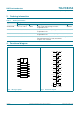
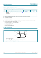
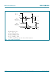
V
M
= 1.5 V at V
CC
2.7 V.
V
M
=0.5 V
CC
at V
CC
<2.7V.
V
X
= V
OL
+ 0.3 V at V
CC
2.7 V;
V
X
= V
OL
+ 0.15 V at V
CC
<2.7V;
V
Y
= V
OH
0.3 V at V
CC
2.7 V;
V
Y
= V
OH
0.15 V at V
CC
< 2.7 V.
V
OL
and V
OH
are typical output voltage levels that occur with the output load.
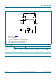
Fig 6. 3-state enable and disable times
mna902
t
PLZ
t
PHZ
outputs
disabled
outputs
enabled
V
Y
V
X
outputs
enabled
output
LOW-to-OFF
OFF-to-LOW
output
HIGH-to-OFF
OFF-to-HIGH
OEn input
V
OL
V
OH
V
CC
V
I
V
M
GND
GND
t
PZL
t
PZH
V
M
V
M