
Datasheet


74LVC74A All information provided in this document is subject to legal disclaimers. © NXP B.V. 2012. All rights reserved.
Product data sheet Rev. 7 — 20 November 2012 11 of 19
NXP Semiconductors
74LVC74A
Dual D-type flip-flop with set and reset; positive-edge trigger
Test data is given in Table 10.
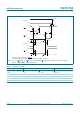
Definitions for test circuit:
R
L
= Load resistance.
C
L
= Load capacitance including jig and probe capacitance.
R
T
= Termination resistance should be equal to output impedance Z
o
of the pulse generator.
Fig 9. Load circuitry for switching times
V
M
V
M
t
W
t
W
10 %
90 %
0 V
V
I
V
I
negative
pulse
positive
pulse
0 V
V
M
V
M
90 %
10 %
t
f
t
r
t
r
t
f
001aaf615
V
CC
V
I
V
O
DUT
C
L
R
T
R
L
PULSE
GENERATOR
Table 10. Test data
Supply voltage Input Load V
EXT
V
CC
V
I
t
r
, t
f
C
L
R
L
t
PLH
, t
PHL
t
PLZ
, t
PZL
t
PHZ
, t
PZH
1.2 V V
CC
2 ns 30 pF 1 k open 2 V
CC
GND
1.65 V to 1.95 V V
CC
2 ns 30 pF 1 k open 2 V
CC
GND
2.3 V to 2.7 V V
CC
2 ns 30 pF 500 open 2 V
CC
GND
2.7V 2.7V 2.5 ns 50 pF 500 open 2 V
CC
GND
3.0Vto3.6V 2.7V 2.5 ns 50 pF 500 open 2 V
CC
GND