
Datasheet

74LVC74A All information provided in this document is subject to legal disclaimers. © NXP B.V. 2012. All rights reserved.
Product data sheet Rev. 7 — 20 November 2012 9 of 19
NXP Semiconductors
74LVC74A
Dual D-type flip-flop with set and reset; positive-edge trigger
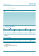
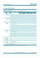
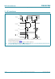
11. AC waveforms
The shaded areas indicate when the input is permitted to change for predictable output performance.
Measurement points are given in Table 9
.
V
OL
and V
OH
are typical output voltage levels that occur with the output load.
Fig 7. The clock input (nCP) to output (nQ, nQ) propagation delays, the clock pulse width, the nD to nCP set-up,
the nCP to nD hold times, and the maximum frequency
mna422
t
h
t
su
t
h
t
PHL
t
PHL
t
W
t
PLH
t
PLH
t
su
1/f
max
V
M
V
M
V
M
V
M
V
I
GND
V
I
GND
nCP input
nD input
V
OH
V
OL
nQ output
V
OH
V
OL
nQ output