
Datasheet


1. General description
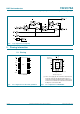
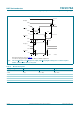
The 74LVC74A is a dual edge triggered D-type flip-flop with individual data (nD) inputs,
clock (nCP) inputs, set (nS
D) and (nRD) inputs, and complementary nQ and nQ outputs.
The set and reset are asynchronous active LOW inputs and operate independently of the
clock input. Information on the data input is transferred to the nQ output on the
LOW-to-HIGH transition of the clock pulse. The nD inputs must be stable one set-up time
prior to the LOW-to-HIGH clock transition, for predictable operation.
Schmitt trigger action at all inputs makes the circuit highly tolerant of slower input rise and
fall times.
2. Features and benefits
5 V tolerant inputs for interlacing with 5 V logic
Wide supply voltage range from 1.2 V to 3.6 V
CMOS low power consumption
Direct interface with TTL levels
Complies with JEDEC standard:
JESD8-7A (1.65 V to 1.95 V)
JESD8-5A (2.3 V to 2.7 V)
JESD8-C/JESD36 (2.7 V to 3.6 V)
ESD protection:
HBM JESD22-A114F exceeds 2000 V
MM JESD22-A115-B exceeds 200 V
CDM JESD22-C101E exceeds 1000 V
Specified from 40 C to +85 C and 40 C to +125 C
74LVC74A
Dual D-type flip-flop with set and reset; positive-edge trigger
Rev. 7 — 20 November 2012 Product data sheet