
Datasheet


74LVC74A All information provided in this document is subject to legal disclaimers. © NXP B.V. 2012. All rights reserved.
Product data sheet Rev. 7 — 20 November 2012 3 of 19
NXP Semiconductors
74LVC74A
Dual D-type flip-flop with set and reset; positive-edge trigger
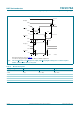
5. Pinning information
5.1 Pinning
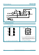
Fig 4. Logic diagram for one flip-flop
mna421
SD
CP
RD
D
C
C
Q
C
C
C
C
C
C
Q
C
C
(1) This is not a supply pin. The substrate is attached to this
pad using conductive die attach material. There is no
electrical or mechanical requirement to solder this pad.
However, if it is soldered, the solder land should remain
floating or be connected to GND.
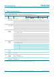
Fig 5. Pin configuration for SO14 and (T)SSOP14 Fig 6. Pin configuration for DHVQFN14
74
1RD V
CC
1D 2RD
1CP 2D
1SD 2CP
1Q 2SD
1Q 2Q
GND 2Q
001aad106
1
2
3
4
5
6
7 8
10
9
12
11
14
13
001aad107
74
Transparent top view
1Q 2Q
1Q 2SD
1SD 2CP
1CP 2D
2RD1D
GND
(1)
GND
2Q
1RD
V
CC
6 9
5 10
4 11
3 12
2 13
7
8
1
14
terminal 1
index area