
Datasheet


74LVC74A All information provided in this document is subject to legal disclaimers. © NXP B.V. 2012. All rights reserved.
Product data sheet Rev. 7 — 20 November 2012 4 of 19
NXP Semiconductors
74LVC74A
Dual D-type flip-flop with set and reset; positive-edge trigger
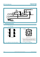
5.2 Pin description
6. Functional description
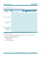
[1] H = HIGH voltage level
L = LOW voltage level
X = don’t care
[1] H = HIGH voltage level
L = LOW voltage level
= LOW-to-HIGH transition
Q
n+1
= state after the next LOW-to-HIGH CP transition
X = don’t care
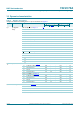
Table 2. Pin description
Symbol Pin Description
1R
D 1 asynchronous reset-direct input (active LOW)
1D 2 data input
1CP 3 clock input (LOW-to-HIGH, edge-triggered)
1S
D 4 asynchronous set-direct input (active LOW)
1Q 5 true output
1Q
6 complement output
GND 7 ground (0 V)
2Q
8 complement output
2Q 9 true output
2S
D 10 asynchronous set-direct input (active LOW)
2CP 11 clock input (LOW-to-HIGH, edge-triggered)
2D 12 data input
2R
D 13 asynchronous reset-direct input (active LOW)
V
CC
14 supply voltage
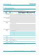
Table 3. Function table
[1]
Input Output
nSD nRD nCP nD nQ nQ
LHXXHL
HLXXLH
LLXXHH
Table 4. Function table
[1]
Input Output
nSD nRD nCP nD nQ
n+1
nQ
n+1
HH LLH
HH HHL