
Datasheet

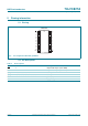
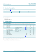
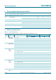

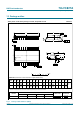
Table Of Contents
- 1. General description
- 2. Features and benefits
- 3. Ordering information
- 4. Functional diagram
- 5. Pinning information
- 6. Functional description
- 7. Limiting values
- 8. Recommended operating conditions
- 9. Static characteristics
- 10. Dynamic characteristics
- 11. Waveforms
- 12. Package outline
- 13. Abbreviations
- 14. Revision history
- 15. Legal information
- 16. Contact information
- 17. Contents

74LVC827A All information provided in this document is subject to legal disclaimers. © NXP B.V. 2011. All rights reserved.
Product data sheet Rev. 4 — 25 November 2011 4 of 16
NXP Semiconductors
74LVC827A
10-bit buffer/line driver with 5 V tolerant inputs/outputs; 3-state
6. Functional description
[1] H = HIGH voltage level
L = LOW voltage level
X = don’t care
Z = high-impedance OFF-state
7. Limiting values
[1] The minimum input voltage ratings may be exceeded if the input current ratings are observed.
[2] The output voltage ratings may be exceeded if the output current ratings are observed.
[3] SO24 package: P
tot
derates linearly with 8 mW/K above 70 C.
(T)SSOP24 package: P
tot
derates linearly with 5.5 mW/K above 60 C.
Table 3. Function table
[1]
Control Input Output
OE1 OE2 An Yn
LLLL
LLHH
XHXZ
HXXZ
Table 4. Limiting values
In accordance with the Absolute Maximum Rating System (IEC 60134). Voltages are referenced to GND (ground = 0 V).
Symbol Parameter Conditions Min Max Unit
V
CC
supply voltage 0.5 +6.5 V
V
I
input voltage
[1]
0.5 +6.5 V
V
O
output voltage output HIGH or LOW state
[2]
0.5 V
CC
+ 0.5 V
output 3-state
[2]
0.5 +6.5 V
I
IK
input clamping current V
I
<0V 50 - mA
I
OK
output clamping current V
O
>V
CC
or V
O
<0V - 50 mA
I
O
output current V
O
= 0 V to V
CC
- 50 mA
I
CC
supply current - 100 mA
I
GND
ground current 100 - mA
T
stg
storage temperature 65 +150 C
P
tot
total power dissipation T
amb
= 40 C to +125 C
[3]
500 mW