
Datasheet

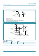

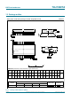
Table Of Contents
- 1. General description
- 2. Features and benefits
- 3. Ordering information
- 4. Functional diagram
- 5. Pinning information
- 6. Functional description
- 7. Limiting values
- 8. Recommended operating conditions
- 9. Static characteristics
- 10. Dynamic characteristics
- 11. Waveforms
- 12. Package outline
- 13. Abbreviations
- 14. Revision history
- 15. Legal information
- 16. Contact information
- 17. Contents
74LVC827A All information provided in this document is subject to legal disclaimers. © NXP B.V. 2011. All rights reserved.
Product data sheet Rev. 4 — 25 November 2011 9 of 16
NXP Semiconductors
74LVC827A
10-bit buffer/line driver with 5 V tolerant inputs/outputs; 3-state
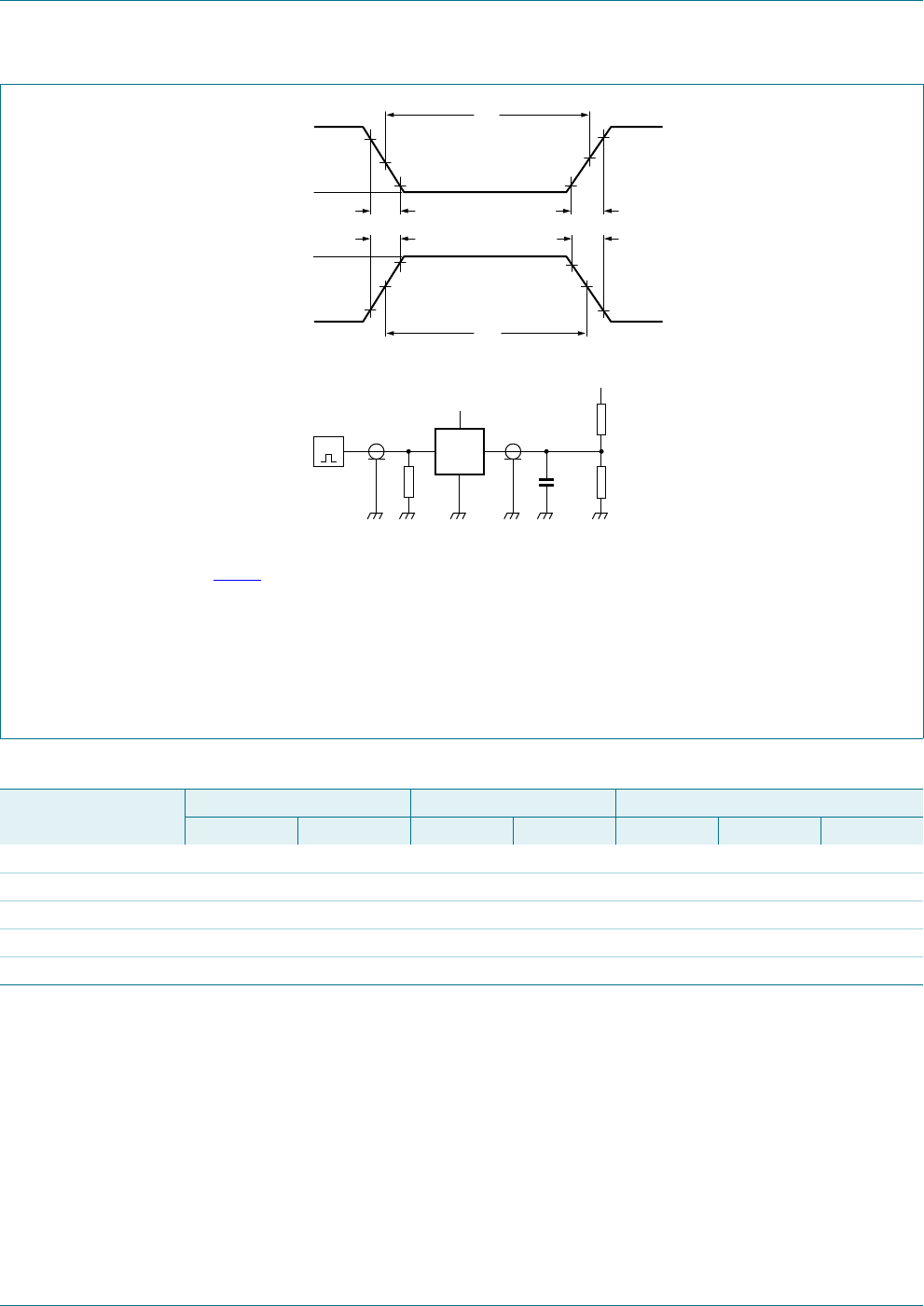
Test data is given in Table 9.
Definitions for test circuit:
R
L
= Load resistance.
C
L
= Load capacitance including jig and probe capacitance.
R
T
= Termination resistance should be equal to output impedance Z
o
of the pulse generator.
V
EXT
= External voltage for measuring switching times.
Fig 6. Test circuit for measuring switching times
V
M
V
M
t
W
t
W
10 %
90 %
0 V
V
I
V
I
negative
pulse
positive
pulse
0 V
V
M
V
M
90 %
10 %
t
f
t
r
t
r
t
f
001aae331
V
EXT
V
CC
V
I
V
O
DUT
C
L
R
T
R
L
R
L
G
Table 9. Test data
Supply voltage Input Load V
EXT
V
I
t
r
, t
f
C
L
R
L
t
PLH
, t
PHL
t
PLZ
, t
PZL
t
PHZ
, t
PZH
1.2 V V
CC
2 ns 30 pF 1 k open 2 V
CC
GND
1.65 V to 1.95 V V
CC
2 ns 30 pF 1 k open 2 V
CC
GND
2.3 V to 2.7 V V
CC
2 ns 30 pF 500 open 2 V
CC
GND
2.7V 2.7V 2.5 ns 50 pF 500 open 2 V
CC
GND
3.0Vto3.6V 2.7V 2.5 ns 50 pF 500 open 2 V
CC
GND