
Datasheet
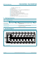
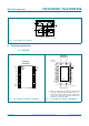


Table Of Contents
- 1. General description
- 2. Features and benefits
- 3. Ordering information
- 4. Functional diagram
- 5. Pinning information
- 6. Functional description
- 7. Limiting values
- 8. Recommended operating conditions
- 9. Static characteristics
- 10. Dynamic characteristics
- 11. Waveforms
- 12. Typical propagation delay characteristics
- 13. Application information
- 14. Package outline
- 15. Abbreviations
- 16. Revision history
- 17. Legal information
- 18. Contact information
- 19. Contents

1. General description
The 74LVC8T245; 74LVCH8T245 are 8-bit dual supply translating transceivers with
3-state outputs that enable bidirectional level translation. They feature two data
input-output ports (pins An and Bn), a direction control input (DIR), an output enable input
(OE
) and dual supply pins (V
CC(A)
and V
CC(B)
). Both V
CC(A)
and V
CC(B)
can be supplied at
any voltage between 1.2 V and 5.5 V making the device suitable for translating between
any of the low voltage nodes (1.2 V, 1.5 V, 1.8 V, 2.5 V, 3.3 V and 5.0 V). Pins An, OE
and
DIR are referenced to V
CC(A)
and pins Bn are referenced to V
CC(B)
. A HIGH on DIR allows
transmission from An to Bn and a LOW on DIR allows transmission from Bn to An. The
output enable input (OE
) can be used to disable the outputs so the buses are effectively
isolated.
The devices are fully specified for partial power-down applications using I
OFF
. The I
OFF
circuitry disables the output, preventing any damaging backflow current through the
device when it is powered down. In suspend mode when either V
CC(A)
or V
CC(B)
are at
GND level, both A port and B port are in the high-impedance OFF-state.
Active bus hold circuitry in the 74LVCH8T245 holds unused or floating data inputs at a
valid logic level.
2. Features and benefits
Wide supply voltage range:
V
CC(A)
: 1.2 V to 5.5 V
V
CC(B)
: 1.2 V to 5.5 V
High noise immunity
Complies with JEDEC standards:
JESD8-7 (1.2 V to 1.95 V)
JESD8-5 (1.8 V to 2.7 V)
JESD8C (2.7 V to 3.6 V)
JESD36 (4.5 V to 5.5 V)
ESD protection:
HBM JESD22-A114F Class 3A exceeds 4000 V
MM JESD22-A115-B exceeds 200 V
CDM JESD22-C101E exceeds 1000 V
Maximum data rates:
420 Mbps (3.3 V to 5.0 V translation)
210 Mbps (translate to 3.3 V))
140 Mbps (translate to 2.5 V)
75 Mbps (translate to 1.8 V)
74LVC8T245; 74LVCH8T245
8-bit dual supply translating transceiver; 3-state
Rev. 3 — 12 December 2011 Product data sheet