
Datasheet

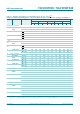


Table Of Contents
- 1. General description
- 2. Features and benefits
- 3. Ordering information
- 4. Functional diagram
- 5. Pinning information
- 6. Functional description
- 7. Limiting values
- 8. Recommended operating conditions
- 9. Static characteristics
- 10. Dynamic characteristics
- 11. Waveforms
- 12. Typical propagation delay characteristics
- 13. Application information
- 14. Package outline
- 15. Abbreviations
- 16. Revision history
- 17. Legal information
- 18. Contact information
- 19. Contents

74LVC_LVCH8T245 All information provided in this document is subject to legal disclaimers. © NXP B.V. 2011. All rights reserved.
Product data sheet Rev. 3 — 12 December 2011 12 of 28
NXP Semiconductors
74LVC8T245; 74LVCH8T245
8-bit dual supply translating transceiver; 3-state
[1] t
pd
is the same as t
PLH
and t
PHL
; t
dis
is the same as t
PLZ
and t
PHZ
; t
en
is the same as t
PZL
and t
PZH
.
Table 12. Dynamic characteristics for temperature range 40 C to +125 C
[1]
Voltages are referenced to GND (ground = 0 V); for test circuit see Figure 7; for wave forms see Figure 5 and Figure 6.
Symbol Parameter Conditions V
CC(B)
Unit
1.5 V 0.1 V 1.8 V 0.15 V 2.5 V 0.2 V 3.3 V 0.3 V 5.0 V 0.5 V
Min Max Min Max Min Max Min Max Min Max
V
CC(A)
= 1.5 V 0.1 V
t
pd
propagation
delay
An to Bn 1.7 32 1.7 27 1.3 21 1.0 18 0.8 16 ns
Bn to An 0.9 32 0.9 30 0.8 28 0.7 28 0.7 26 ns
t
dis
disable time OE to An 1.5 34 1.5 34 1.5 34 1.5 34 1.4 34 ns
OE
to Bn 2.4 41 2.4 40 1.9 18 1.7 17 1.3 15 ns
t
en
enable time OE to An 0.4 40 0.4 40 0.4 40 0.4 40 0.4 40 ns
OE
to Bn 1.8 43 1.8 41 1.5 22 1.2 18 0.9 16 ns
V
CC(A)
= 1.8 V 0.15 V
t
pd
propagation
delay
An to Bn 1.7 30 1.7 25.9 1.3 13.2 1.0 11.4 0.8 11.1 ns
Bn to An 0.9 27 0.9 28.8 0.8 27.6 0.7 27.4 0.7 27.4 ns
t
dis
disable time OE to An 1.5 34 1.5 33.6 1.5 33.4 1.5 33.3 1.4 33.2 ns
OE
to Bn 2.4 40 2.4 36.2 1.9 17.1 1.7 16.0 1.3 14.3 ns
t
en
enable time OE to An 0.4 28 0.4 28 0.4 27.8 0.4 27.7 0.4 27.7 ns
OE
to Bn 1.8 41 1.8 40 1.5 20 1.2 16.6 0.9 14.8 ns
V
CC(A)
= 2.5 V 0.2 V
t
pd
propagation
delay
An to Bn 1.5 28 1.5 25.4 1.2 13 0.8 10.2 0.6 8.8 ns
Bn to An 1.2 23 1.2 13.3 1.0 13.1 1.0 12.9 0.9 12.8 ns
t
dis
disable time OE to An 1.4 13 1.4 13 1.4 13 1.4 13 1.4 13 ns
OE
to Bn 2.3 37 2.3 33.6 1.8 15 1.7 14.3 0.9 10.9 ns
t
en
enable time OE to An 1.0 17.2 1.0 17.2 1.0 17.3 1.0 17.2 1.0 17.3 ns
OE
to Bn 1.7 38 1.7 32.2 1.5 18.1 1.2 14.1 1.0 11.2 ns
V
CC(A)
= 3.3 V 0.3 V
t
pd
propagation
delay
An to Bn 1.5 28 1.5 25.2 1.1 12.8 0.8 10.3 0.5 10.4 ns
Bn to An 0.8 18 0.8 11.2 0.8 10.2 0.7 10.1 0.6 10 ns
t
dis
disable time OE to An 1.6 12.2 1.6 12.2 1.6 12.2 1.6 12.2 1.6 12.2 ns
OE
to Bn 2.1 36 2.1 33 1.7 14.3 1.5 12.6 0.8 10.3 ns
t
en
enable time OE to An 0.8 14.1 0.8 14.1 0.8 13.6 0.8 13.2 0.8 13.6 ns
OE
to Bn 1.8 37 1.8 31.7 1.4 18.4 1.1 12.9 0.9 10.9 ns
V
CC(A)
= 5.0 V 0.5 V
t
pd
propagation
delay
An to Bn 1.5 26 1.5 25.4 1.0 12.8 0.7 10 0.4 8.2 ns
Bn to An 0.7 16 0.7 11 0.4 8.8 0.3 8.5 0.3 8.3 ns
t
dis
disable time OE to An 0.3 9.4 0.3 9.4 0.3 9.4 0.3 9.4 0.3 9.4 ns
OE
to Bn 2.0 36 2.0 32.7 1.6 13.7 1.4 12 0.7 9.7 ns
t
en
enable time OE to An 0.7 10.9 0.7 10.9 0.7 10.9 0.7 10.9 0.7 10.9 ns
OE
to Bn 1.5 37 1.5 31.6 1.3 18.4 1.0 13.7 0.9 10.7 ns