
Datasheet

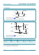
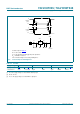

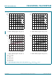


Table Of Contents
- 1. General description
- 2. Features and benefits
- 3. Ordering information
- 4. Functional diagram
- 5. Pinning information
- 6. Functional description
- 7. Limiting values
- 8. Recommended operating conditions
- 9. Static characteristics
- 10. Dynamic characteristics
- 11. Waveforms
- 12. Typical propagation delay characteristics
- 13. Application information
- 14. Package outline
- 15. Abbreviations
- 16. Revision history
- 17. Legal information
- 18. Contact information
- 19. Contents
74LVC_LVCH8T245 All information provided in this document is subject to legal disclaimers. © NXP B.V. 2011. All rights reserved.
Product data sheet Rev. 3 — 12 December 2011 16 of 28
NXP Semiconductors
74LVC8T245; 74LVCH8T245
8-bit dual supply translating transceiver; 3-state
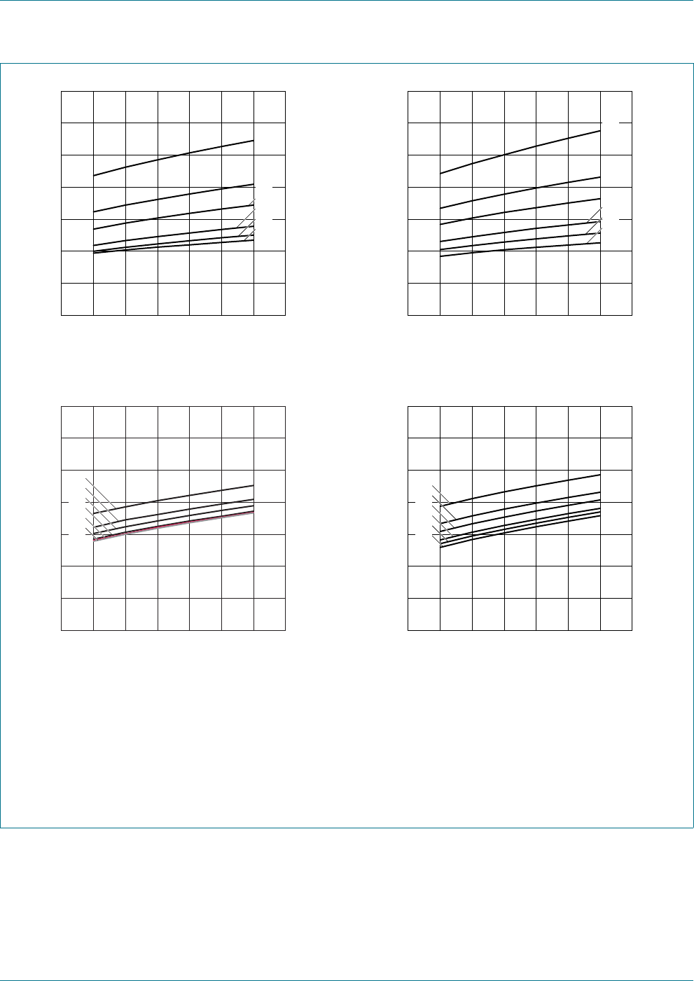
a. HIGH to LOW propagation delay (A to B) b. LOW to HIGH propagation delay (A to B)
c. HIGH to LOW propagation delay (B to A) d. LOW to HIGH propagation delay (B to A)
(1) V
CC(B)
= 1.2 V.
(2) V
CC(B)
= 1.5 V.
(3) V
CC(B)
= 1.8 V.
(4) V
CC(B)
= 2.5 V.
(5) V
CC(B)
= 3.3 V.
(6) V
CC(B)
= 5.0 V.
Fig 9. Typical propagation delay versus load capacitance; T
amb
= 25 C; V
CC(A)
=1.5V
C
L
(pF)
35255302010015
001aal272
6
2
10
14
4
8
12
t
PHL
(ns)
0
(3)
(4)
(5)
(6)
(1)
(2)
C
L
(pF)
35255302010015
001aal273
6
2
10
14
4
8
12
t
PLH
(ns)
0
(3)
(4)
(5)
(6)
(1)
(2)
C
L
(pF)
35255302010015
001aal274
6
2
10
14
4
8
12
t
PHL
(ns)
0
(1)
(2)
(3)
(4)
(5)
(6)
C
L
(pF)
35255302010015
001aal275
6
2
10
14
4
8
12
t
PLH
(ns)
0
(1)
(2)
(3)
(4)
(5)
(6)