
Datasheet


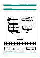
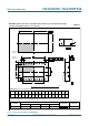
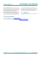
Table Of Contents
- 1. General description
- 2. Features and benefits
- 3. Ordering information
- 4. Functional diagram
- 5. Pinning information
- 6. Functional description
- 7. Limiting values
- 8. Recommended operating conditions
- 9. Static characteristics
- 10. Dynamic characteristics
- 11. Waveforms
- 12. Typical propagation delay characteristics
- 13. Application information
- 14. Package outline
- 15. Abbreviations
- 16. Revision history
- 17. Legal information
- 18. Contact information
- 19. Contents

74LVC_LVCH8T245 All information provided in this document is subject to legal disclaimers. © NXP B.V. 2011. All rights reserved.
Product data sheet Rev. 3 — 12 December 2011 22 of 28
NXP Semiconductors
74LVC8T245; 74LVCH8T245
8-bit dual supply translating transceiver; 3-state
13.2 Bidirectional logic level-shifting application
Figure 15 shows the 74LVC8T245; 74LVCH8T245 being used in a bidirectional logic
level-shifting application.
Table 16 gives a sequence that will illustrate data transmission from system-1 to system-2
and then from system-2 to system-1.
[1] H = HIGH voltage level; L = LOW voltage level; Z = high-impedance OFF-state.
13.3 Power-up considerations
The device is designed such that no special power-up sequence is required other than
GND being applied first.
Schematic given for one channel.
Pull-up or pull-down only needed for 74LVC8T245.
Fig 15. Bidirectional logic level-shifting application
Table 16. Description bidirectional logic level-shifting application
[1]
State DIR CTRL OE I/O-1 I/O-2 Description
1 H L output input system-1 data to system-2
2 H H Z Z system-2 is getting ready to send data to
system-1. I/O-1 and I/O-2 are disabled. The
bus-line state depends on bus hold.
3 L H Z Z DIR bit is set LOW. I/O-1 and I/O-2 still are
disabled. The bus-line state depends on bus
hold.
4 L L input output system-2 data to system-1
001aak439
PULL-UP/DOWN PULL-UP/DOWN
74LVC8T245
74LVCH8T245
V
CC1
V
CC1
V
CC2
V
CC2
I/O-2I/O-1
DIR CTRL
system-2system-1
V
CC(A)
V
CC(B)
GND DIR
B
OE
A
OE
Table 17. Typical total supply current (I
CC(A)
+ I
CC(B)
)
V
CC(A)
V
CC(B)
Unit
0 V 1.8 V 2.5 V 3.3 V 5.0 V
0 V0 < 1< 1< 1< 1A
1.8 V < 1 < 2 < 2 < 2 2 A
2.5 V < 1 < 2 < 2 < 2 < 2 A
3.3 V < 1 < 2 < 2 < 2 < 2 A
5.0 V < 1 2 < 2 < 2 < 2 A