
Datasheet
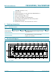
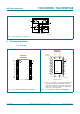
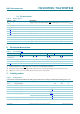
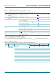
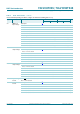


Table Of Contents
- 1. General description
- 2. Features and benefits
- 3. Ordering information
- 4. Functional diagram
- 5. Pinning information
- 6. Functional description
- 7. Limiting values
- 8. Recommended operating conditions
- 9. Static characteristics
- 10. Dynamic characteristics
- 11. Waveforms
- 12. Typical propagation delay characteristics
- 13. Application information
- 14. Package outline
- 15. Abbreviations
- 16. Revision history
- 17. Legal information
- 18. Contact information
- 19. Contents

74LVC_LVCH8T245 All information provided in this document is subject to legal disclaimers. © NXP B.V. 2011. All rights reserved.
Product data sheet Rev. 3 — 12 December 2011 3 of 28
NXP Semiconductors
74LVC8T245; 74LVCH8T245
8-bit dual supply translating transceiver; 3-state
5. Pinning information
5.1 Pinning
Fig 2. Logic diagram (one channel)
001aai473
to other seven channels
DIR
A1
V
CC(A)
V
CC(B)
OE
B1
(1) This is not a supply pin, the substrate is attached to this
pad using conductive die attach material. There is no
electrical or mechanical requirement to solder this pad
however if it is soldered the solder land should remain
floating or be connected to GND.
Fig 3. Pin configuration SOT355-1 (TSSOP24) Fig 4. Pin configuration SOT815-1 (DHVQFN24)
74LVC8T245
74LVCH8T245
V
CC(A)
V
CC(B)
DIR V
CC(B)
A1 OE
A2 B1
A3 B2
A4 B3
A5 B4
A6 B5
A7 B6
A8 B7
GND B8
GND GND
001aak436
1
2
3
4
5
6
7
8
9
10
11
12
14
13
16
15
18
17
20
19
22
21
24
23
001aak437
74LVC8T245
74LVCH8T245
Transparent top view
B8
A8
GND
B7
A7 B6
A6 B5
A5 B4
A4 B3
A3 B2
A2 B1
A1 OE
DIR V
CC(B)
GND
GND
V
CC(A)
V
CC(B)
11 14
10 15
9 16
8 17
7 18
6 19
5 20
4 21
3 22
2 23
12
13
1
24
terminal 1
index area
GND
(1)