
Datasheet


74LVT14_2 © NXP B.V. 2008. All rights reserved.
Product data sheet Rev. 02 — 25 April 2008 3 of 13
NXP Semiconductors
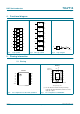
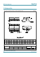
74LVT14
3.3 V hex inverter Schmitt trigger
5.2 Pin description
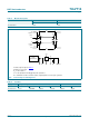
6. Functional description
[1] H = HIGH voltage level;
L = LOW voltage level.
7. Limiting values
[1] The performance capability of a high-performance integrated circuit in conjunction with its thermal environment can create junction
temperatures which are detrimental to reliability. The maximum junction temperature of this integrated circuit should not exceed 150 °C.
[2] The input and output negative voltage ratings may be exceeded if the input and output clamp current ratings are observed.
[3] For SO14 packages: above 70 °C derate linearly with 8 mW/K.
For SSOP14 and TSSOP14 packages: above 60 °C derate linearly with 5.5 mW/K.
For DHVQFN14 packages: above 60 °C derate linearly with 4.5 mW/K.
Table 2. Pin description
Symbol Pin Description
1A to 6A 1, 3, 5, 9, 11, 13 data input
1Y to 6Y 2, 4, 6, 8, 10, 12 data output
GND 7 ground (0 V)
V
CC
14 positive supply voltage
Table 3. Function selection
Inputs Output
nA nY
LH
HL
Table 4. Limiting values
[1]
In accordance with the Absolute Maximum Rating System (IEC 60134). Voltages are referenced to GND (ground = 0 V).
Symbol Parameter Conditions Min Max Unit
V
CC
supply voltage −0.5 +4.6 V
V
I
input voltage
[2]
−0.5 +7.0 V
V
O
output voltage output in OFF or HIGH state
[2]
−0.5 +7.0 V
I
IK
input clamping current V
I
< 0 V −50 - mA
I
OK
output clamping current V
O
< 0 V −50 - mA
I
O
output current output in LOW state - 64 mA
output in HIGH state −32 - mA
T
stg
storage temperature −65 +150 °C
T
j
junction temperature +150 °C
P
tot
total power dissipation T
amb
= −40 °C to +85 °C
[3]
500 mW