
Datasheet


74LVT14_2 © NXP B.V. 2008. All rights reserved.
Product data sheet Rev. 02 — 25 April 2008 4 of 13
NXP Semiconductors
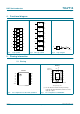
74LVT14
3.3 V hex inverter Schmitt trigger
8. Recommended operating conditions
9. Static characteristics
[1] All typical values are measured at V
CC
= 3.3 V (unless stated otherwise) and T
amb
=25°C.
[2] This is the increase in the supply current for each input at the specified voltage level other than V
CC
or GND.
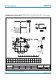
Table 5. Recommended operating conditions
Symbol Parameter Conditions Min Typ Max Unit
V
CC
supply voltage 2.7 - 3.6 V
V
I
input voltage 0 - 5.5 V
I
OH
HIGH-level output current −20 - - mA
I
OL
LOW-level output current - - 32 mA
T
amb
ambient temperature in free air −40 - +85 °C
∆t/∆V input transition rise and fall rate output enabled 0 - 10 ns/V
Table 6. Static characteristics
At recommended operating conditions. Voltages are referenced to GND (ground = 0 V).
Symbol Parameter Conditions −40 °C to +85 °C Unit
Min Typ
[1]
Max
V
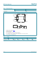
T+
positive-going threshold voltage V
CC
= 3.3 V; see Figure 7 1.5 1.7 2.0 V
V
T−
negative-going threshold voltage V
CC
= 3.3 V; see Figure 7 0.9 1.1 1.3 V
V
H
hysteresis voltage V
CC
= 3.3 V; see Figure 7 0.4 0.6 - V
V
IK
input clamping voltage V
CC
= 2.7 V; I
IK
= –18 mA −1.2 - - V
V
IH
HIGH-level input voltage 2.0 - - V
V
IL
LOW-level input voltage - - 0.8
V
OH
HIGH-level output voltage V
CC
= 2.7 V to 3.6 V; I
OH
= −100 µAV
CC
− 0.2 - - V
V
CC
= 2.7 V; I
OH
= −6 mA 2.4 - - V
V
CC
= 3.0 V; I
OH
= −20 mA 2.0 - - V
V
OL
LOW-level output voltage V
CC
= 2.7 V; I
OL
= 100 µA - - 0.2 V
V
CC
= 2.7 V; I
OL
= 24 mA - - 0.5 V
V
CC
= 3.0 V; I
OL
= 32 mA - - 0.5 V
I
I
input leakage current V
CC
= 0 V or 3.6 V; V
I
= 5.5 V - - 10 µA
V
CC
= 3.6 V; V
I
=V
CC
or GND - - ±1 µA
I
OFF
power-off leakage current V
CC
= 0 V; V
I
or V
O
= 0 V to 4.5 V - - ±100 µA
I
CC
supply current V
CC
= 3.6 V; V
I
= GND or V
CC
; I
O
=0A
outputs HIGH - - 0.02 mA
outputs LOW - 1.5 3 mA
∆I
CC
additional supply current per input pin; V
CC
= 3.0 V to 3.6 V;
one input = V
CC
− 0.6 V
other inputs at V
CC
or GND
[2]
- - 0.2 mA
C
I
input capacitance V
I
= 0 V or 3.0 V - 3 - pF