
Datasheet


74LVT14_2 © NXP B.V. 2008. All rights reserved.
Product data sheet Rev. 02 — 25 April 2008 5 of 13
NXP Semiconductors
74LVT14
3.3 V hex inverter Schmitt trigger
10. Dynamic characteristics
[1] Typical values are measured at T
amb
=25°C and V
CC
= 3.3 V.
11. Waveforms
Table 7. Dynamic characteristics
Voltages are referenced to GND (ground = 0 V). For test circuit see Figure 8.
Symbol Parameter Conditions −40 °C to +85 °C Unit
Min Typ
[1]
Max
t
PLH
LOW to HIGH propagation delay nA to nY
V
CC
= 2.7 V - - 6.9 ns
V
CC
= 3.3 V + 0.3 V 1.0 3.8 5.7 ns
t
PHL
HIGH to LOW propagation delay nA to nY
V
CC
= 2.7 V - - 4.1 ns
V
CC
= 3.3 V + 0.3 V 1.0 3.2 4.5 ns
See Table 8 for measurement points.
V
OL
and V
OH
are typical output voltage levels that occur with the output load.
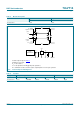
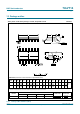
Fig 6. nA Input to nY output propagation delays
mna344
t
PHL
t
PLH
V
M
V
M
V
M
V
M
nA input
nY output
GND
V
I
V
OH
V
OL
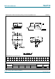
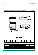
a. Transfer characteristics b. Voltage levels
Fig 7. Definition of V
T+
, V
T−
and V
H
mna207
V
O
V
I
V
H
V
T+
V
T−
mna208
V
O
V
I
V
H
V
T+
V
T−