
Datasheet


74LVT14_2 © NXP B.V. 2008. All rights reserved.
Product data sheet Rev. 02 — 25 April 2008 6 of 13
NXP Semiconductors
74LVT14
3.3 V hex inverter Schmitt trigger
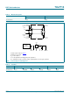
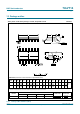
Table 8. Measurement points
V
CC
Input Output
V
M
V
M
2.7 V to 3.6 V 1.5 V 1.5 V
Test data is given in given in Table 9.
Definitions for test circuit:
R
L
= Load resistance;
C
L
= Load capacitance including jig and probe capacitance;
R
T
= Termination resistance should be equal to output impedance Z
o
of the pulse generator.
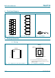
Fig 8. Load circuitry for switching times
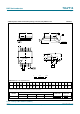
V
M
V
M
t
W
t
W
10 %
90 %
0 V
V
I
V
I
negative
pulse
positive
pulse
0 V
V
M
V
M
90 %
10 %
t
f
t
r
t
r
t
f
001aaf615
V
CC
V
I
V
O
DUT
C
L
R
T
R
L
PULSE
GENERATOR
Table 9. Test data
Supply Input pulse requirements Load
V
CC
V
I
Repetition rate t
W
t
r
, t
f
R
L
C
L
2.7 V to 3.3 V 2.7 V ≤ 10 MHz 500 ns ≤ 2.5 ns 500 Ω 50 pF