
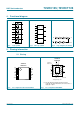
Datasheet


1. General description
The 74VHC125; 74VHCT125 are high-speed Si-gate CMOS devices and are pin
compatible with Low-power Schottky TTL (LSTTL). They are specified in compliance with
JEDEC standard JESD7-A.
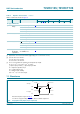
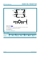
The 74VHC125; 74VHCT125 provides four non-inverting buffer/line drivers with 3-state
outputs. The 3-state outputs (nY) are controlled by the output enable input (nOE). A HIGH
at nOE causes the outputs to assume a high-impedance OFF-state.
The 74VHC125; 74VHCT125 are identical to the 74VHC126; 74VHCT126 but have active
LOW enable inputs.
2. Features
n Balanced propagation delays
n All inputs have a Schmitt-trigger action
n Inputs accepts voltages higher than V
CC
n Input levels:
u The 74VHC125 operates with CMOS logic levels
u The 74VHCT125 operates with TTL logic levels
n ESD protection:
u HBM JESD22-A114E exceeds 2000 V
u MM JESD22-A115-A exceeds 200 V
u CDM JESD22-C101C exceeds 1000 V
n Multiple package options
n Specified from −40 °C to +85 °C and from −40 °C to +125 °C
3. Ordering information
74VHC125; 74VHCT125
Quad buffer/line driver; 3-state
Rev. 02 — 13 October 2009 Product data sheet
Table 1. Ordering information
Type number Package
Temperature range Name Description Version
74VHC125D −40 °C to +125 °C SO14 plastic small outline package; 14 leads;
body width 3.9 mm
SOT108-1
74VHCT125D
74VHC125PW −40 °C to +125 °C TSSOP14 plastic thin shrink small outline package; 14 leads;
body width 4.4 mm
SOT402-1
74VHCT125PW
74VHC125BQ −40 °C to +125 °C DHVQFN14 plastic dual in-line compatible thermal enhanced very
thin quad flat package; no leads; 14 terminals;
body 2.5 × 3 × 0.85 mm
SOT762-1
74VHCT125BQ