
Datasheet


74VHC_VHCT125_2 © NXP B.V. 2009. All rights reserved.
Product data sheet Rev. 02 — 13 October 2009 2 of 15
NXP Semiconductors
74VHC125; 74VHCT125
Quad buffer/line driver; 3-state
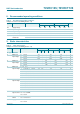
4. Functional diagram
5. Pinning information
5.1 Pinning
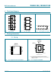
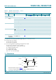
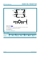
Fig 1. Logic symbol Fig 2. IEC logic symbol Fig 3. Logic diagram (one buffer)
mna228
1A 1Y
2
1
3
1OE
2A 2Y
5
4
6
2OE
3A 3Y
9
10
8
3OE
4A 4Y
12
13
11
4OE
mna229
1
EN1
1
3
2
4
6
5
10
8
9
13
11
12
mna227
nOE
nA
nY
(1) The die substrate is attached to this pad using
conductive die attach material. It can not be used as a
supply pin or input.
Fig 4. Pin configuration SO14 and TSSOP14 Fig 5. Pin configuration DHVQFN14
74VHC125
74VHCT125
1OE V
CC
1A 4OE
1Y 4A
2OE 4Y
2A 3OE
2Y 3A
GND 3Y
001aak044
1
2
3
4
5
6
7
8
10
9
12
11
14
13
001aak045
74VHC125
74VHCT125
Transparent top view
2Y 3A
2A 3OE
2OE 4Y
1Y 4A
1A 4OE
GND
3Y
1OE
V
CC
6 9
5 10
4 11
3 12
2 13
7
8
1
14
terminal 1
index area
GND
(1)