
Datasheet
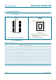

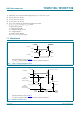
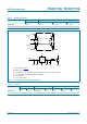
Table Of Contents
- 1. General description
- 2. Features
- 3. Ordering information
- 4. Functional diagram
- 5. Pinning information
- 6. Functional description
- 7. Limiting values
- 8. Recommended operating conditions
- 9. Static characteristics
- 10. Dynamic characteristics
- 11. Waveforms
- 12. Package outline
- 13. Abbreviations
- 14. Revision history
- 15. Legal information
- 16. Contact information
- 17. Contents
1. General description
The 74VHC126; 74VHCT126 are high-speed Si-gate CMOS devices and are pin
compatible with Low-power Schottky TTL (LSTTL). They are specified in compliance with
JEDEC standard No. 7-A.
The 74VHC126; 74VHCT126 provide four non-inverting buffer/line drivers with 3-state
outputs. The 3-state outputs (nY) are controlled by the output enable input (nOE).
A LOW-level at pin nOE causes the outputs to assume a high-impedance OFF-state.
The 74VHC126; 74VHCT126 are identical to the 74VHC125; 74VHCT125 but have active
HIGH output enable inputs.
2. Features
n Balanced propagation delays
n All inputs have Schmitt-trigger action
n Inputs accept voltages higher than V
CC
n Input levels:
u The 74VHC126 operates with CMOS input level
u The 74VHCT126 operates with TTL input level
n ESD protection:
u HBM JESD22-A114E exceeds 2000 V
u MM JESD22-A115-A exceeds 200 V
u CDM JESD22-C101C exceeds 1000 V
n Multiple package options
n Specified from −40 °C to +85 °C and from −40 °C to +125 °C
74VHC126; 74VHCT126
Quad buffer/line driver; 3-state
Rev. 01 — 13 August 2009 Product data sheet