
Datasheet
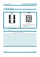

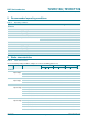
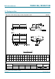
Table Of Contents
- 1. General description
- 2. Features
- 3. Ordering information
- 4. Functional diagram
- 5. Pinning information
- 6. Functional description
- 7. Limiting values
- 8. Recommended operating conditions
- 9. Static characteristics
- 10. Dynamic characteristics
- 11. Waveforms
- 12. Package outline
- 13. Abbreviations
- 14. Revision history
- 15. Legal information
- 16. Contact information
- 17. Contents

74VHC_VHCT126_1 © NXP B.V. 2009. All rights reserved.
Product data sheet Rev. 01 — 13 August 2009 3 of 15
NXP Semiconductors
74VHC126; 74VHCT126
Quad buffer/line driver; 3-state
5. Pinning information
5.1 Pinning
5.2 Pin description
(1) The die substrate is attached to this pad using
conductive die attach material. It can not be used as
a supply pin or input.
Fig 4. Pin configuration SO14 and TSSOP14 Fig 5. Pin configuration DHVQFN14
74VHC126
74VHCT126
1OE V
CC
1A 4OE
1Y 4A
2OE 4Y
2A 3OE
2Y 3A
GND 3Y
001aak056
1
2
3
4
5
6
7 8
10
9
12
11
14
13
001aak076
74VHC126
74VHCT126
Transparent top view
2Y 3A
2A 3OE
2OE 4Y
1Y 4A
1A 4OE
GND
3Y
1OE
V
CC
6 9
5 10
4 11
3 12
2 13
7
8
1
14
terminal 1
index area
GND
(1)
Table 2. Pin description
Symbol Pin Description
1OE 1 output enable input 1 (active HIGH)
1A 2 data input 1
1Y 3 data output 1
2OE 4 output enable input 2 (active HIGH)
2A 5 data input 2
2Y 6 data output 2
GND 7 ground (0 V)
3Y 8 data output 3
3A 9 data input 3
3OE 10 output enable input 3 (active HIGH)
4Y 11 data output 4
4A 12 data input 4
4OE 13 output enable input 4 (active HIGH)
V
CC
14 supply voltage