
Datasheet

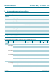
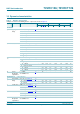
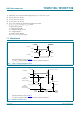
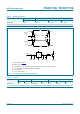
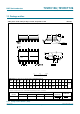
Table Of Contents
- 1. General description
- 2. Features
- 3. Ordering information
- 4. Functional diagram
- 5. Pinning information
- 6. Functional description
- 7. Limiting values
- 8. Recommended operating conditions
- 9. Static characteristics
- 10. Dynamic characteristics
- 11. Waveforms
- 12. Package outline
- 13. Abbreviations
- 14. Revision history
- 15. Legal information
- 16. Contact information
- 17. Contents

74VHC_VHCT126_1 © NXP B.V. 2009. All rights reserved.
Product data sheet Rev. 01 — 13 August 2009 4 of 15
NXP Semiconductors
74VHC126; 74VHCT126
Quad buffer/line driver; 3-state
6. Functional description
[1] H = HIGH voltage state;
L = LOW voltage state;
X = don’t care;
Z = high-impedance OFF-state.
7. Limiting values
[1] The input and output voltage ratings may be exceeded if the input and output current ratings are observed.
[2] For SO14 packages: above 70 °C the value of P
tot
derates linearly at 8 mW/K.
For TSSOP14 packages: above 60 °C the value of P
tot
derates linearly at 5.5 mW/K.
For DHVQFN14 packages: above 60 °C the value of P
tot
derates linearly at 4.5 mW/K.
Table 3. Function table
[1]
Control Input Output
nOE nA nY
HL L
HHH
LXZ
Table 4. Limiting values
In accordance with the Absolute Maximum Rating System (IEC 60134). Voltages are referenced to GND (ground = 0 V).
Symbol Parameter Conditions Min Max Unit
V
CC
supply voltage −0.5 +7.0 V
V
I
input voltage −0.5 +7.0 V
I
IK
input clamping current V
I
< −0.5 V
[1]
−20 - mA
I
OK
output clamping current V
O
< −0.5 V or V
O
> V
CC
+ 0.5 V
[1]
−20 +20 mA
I
O
output current V
O
= −0.5 V to (V
CC
+ 0.5 V) −25 +25 mA
I
CC
supply current - +75 mA
I
GND
ground current −75 - mA
T
stg
storage temperature −65 +150 °C
P
tot
total power dissipation T
amb
= −40 °C to +125 °C
[2]
- 500 mW