
Datasheet

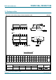
Table Of Contents
- 1. General description
- 2. Features
- 3. Ordering information
- 4. Functional diagram
- 5. Pinning information
- 6. Functional description
- 7. Limiting values
- 8. Recommended operating conditions
- 9. Static characteristics
- 10. Dynamic characteristics
- 11. Waveforms
- 12. Package outline
- 13. Abbreviations
- 14. Revision history
- 15. Legal information
- 16. Contact information
- 17. Contents

74VHC_VHCT126_1 © NXP B.V. 2009. All rights reserved.
Product data sheet Rev. 01 — 13 August 2009 8 of 15
NXP Semiconductors
74VHC126; 74VHCT126
Quad buffer/line driver; 3-state
[1] Typical values are measured at nominal supply voltage (V
CC
= 3.3 V and V
CC
= 5.0 V).
[2] t
pd
is the same as t
PLH
and t
PHL
.
[3] t
en
is the same as t
PZL
and t
PZH
.
[4] t
dis
is the same as t
PLZ
and t
PHZ
.
[5] C
PD
is used to determine the dynamic power dissipation (P
D
in µW).
P
D
=C
PD
× V
CC
2
× f
i
× N+Σ(C
L
× V
CC
2
× f
o
) where:
f
i
= input frequency in MHz;
f
o
= output frequency in MHz;
C
L
= output load capacitance in pF;
V
CC
= supply voltage in V;
N = number of inputs switching;
Σ(C
L
× V
CC
2
× f
o
) = sum of the outputs.
11. Waveforms
Measurement points are given in Table 8.
V
OL
and V
OH
are typical voltage output levels that occur with the output load.
Fig 6. Input to output propagation delays
mna237
t
PHL
t
PLH
V
M
V
M
nA input
nY output
GND
V
I
V
OH
V
OL
Measurement points are given in Table 8.
V
OL
and V
OH
are typical voltage output levels that occur with the output load.
Fig 7. Enable and disable times
mna949
t
PLZ
t
PHZ
outputs
disabled
outputs
enabled
V
Y
V
X
outputs
enabled
output
LOW-to-OFF
OFF-to-LOW
output
HIGH-to-OFF
OFF-to-HIGH
nOE input
V
OL
V
OH
V
CC
V
I
V
M
GND
GND
t
PZL
t
PZH
V
M
V
M