
Datasheet

74VHC_VHCT541_1 © NXP B.V. 2009. All rights reserved.
Product data sheet Rev. 01 — 12 August 2009 9 of 16
NXP Semiconductors
74VHC541; 74VHCT541
Octal buffer/line driver; 3-state
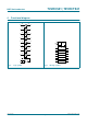
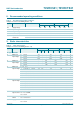
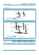
11. Waveforms
Measurement points are given in Table 8.
V
OL
and V
OH
are typical voltage output levels that occur with the output load.
Fig 5. Propagation delay input (An) to output (Yn)
mna901
An input
Yn output
t
PHL
t
PLH
GND
V
I
V
M
V
M
V
OH
V
OL
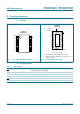
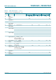
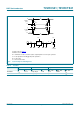
Measurement points are given in Table 8.
V
OL
and V
OH
are typical voltage output levels that occur with the output load.
Fig 6. Enable and disable times
mna902
t
PLZ
t
PHZ
outputs
disabled
outputs
enabled
V
Y
V
X
outputs
enabled
output
LOW-to-OFF
OFF-to-LOW
output
HIGH-to-OFF
OFF-to-HIGH
OEn input
V
OL
V
OH
V
CC
V
I
V
M
GND
GND
t
PZL
t
PZH
V
M
V
M
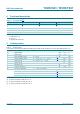
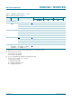
Table 8. Measurement points
Type Input Output
V
M
V
M
V
X
V
Y
74VHC541 0.5V
CC
0.5V
CC
V
OL
+ 0.3 V V
OH
− 0.3 V
74VHCT541 1.5 V 0.5V
CC
V
OL
+ 0.3 V V
OH
− 0.3 V