
Datasheet
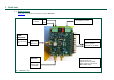
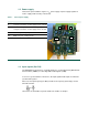

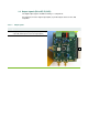
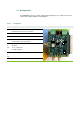


Table 2. Input signals, CMOS Clock
Name Function View
J1 IN connector – Analog input signal (
50Ω
matching)
J2 CLKP connector – Single ended 1.8V CMOS clock input
signal
J3 CLKN connector – Grounded on that demo board
ST7 Clock input format selection. 0: 1.8V CMOS
Table 3. Input signals, LVDS Clock
Name Function View
J1 IN connector – Analog input signal (
50Ω
matching)
J2 CLKP connector – LVDS Clock input, 50 ohms must be
soldered on R7 footprint.
J3 CLKN connector – LVDS complementary Clock input, 50
ohms must be soldered on R8 footprint.
ST7 Clock input format selection. NC: LVDS
J
1
J2
J3
J
1
J2
J3
R
7
R
8
ST
7