ADC1015S series Single 10-bit ADC; 65 Msps, 80 Msps, 105 Msps or 125 Msps with input buffer; CMOS or LVDS DDR digital outputs Rev. 2 — 20 December 2010 Product data sheet 1. General description The ADC1015S is a single channel 10-bit Analog-to-Digital Converter (ADC) optimized for high dynamic performances and low power consumption at sample rates up to 125 Msps.
ADC1015S series NXP Semiconductors Single 10-bit ADC; input buffer; CMOS or LVDS DDR digital outputs 3. Applications Wireless and wired broadband communications Portable instrumentation Imaging systems Digital predistortion loop, power amplifier linearization Spectral analysis Ultrasound equipment Software defined radio 4. Ordering information Table 1.
ADC1015S series NXP Semiconductors Single 10-bit ADC; input buffer; CMOS or LVDS DDR digital outputs 5.
ADC1015S series NXP Semiconductors Single 10-bit ADC; input buffer; CMOS or LVDS DDR digital outputs 6. Pinning information 31 DAV 32 n.c. 33 VDDO 34 OGND 35 OTR 36 SCLK/DFS 37 SDIO/ODS 38 CS 39 SENSE 40 VREF terminal 1 index area 31 DAV 32 n.c. 33 VDDO 34 OGND 35 OTR 36 SCLK/DFS 37 SDIO/ODS 38 CS terminal 1 index area 39 SENSE 40 VREF 6.1 Pinning REFB 1 30 n.c. REFB 1 30 n.c. REFT 2 29 n.c. REFT 2 29 n.c. AGND 3 28 n.c. AGND 3 28 n.c. VCM 4 VCM 4 27 n.c.
ADC1015S series NXP Semiconductors Single 10-bit ADC; input buffer; CMOS or LVDS DDR digital outputs Table 2. Symbol Pin Type [1] Description D9 17 O data output bit 9 (Most Significant Bit (MSB)) D8 18 O data output bit 8 D7 19 O data output bit 7 D6 20 O data output bit 6 D5 21 O data output bit 5 D4 22 O data output bit 4 D3 23 O data output bit 3 D2 24 O data output bit 2 D1 25 O data output bit 1 D0 26 O data output bit 0 (Least Significant Bit (LSB)) n.c.
ADC1015S series NXP Semiconductors Single 10-bit ADC; input buffer; CMOS or LVDS DDR digital outputs Table 3. Pin description …continued (LVDS/DDR) digital outputs) Symbol Pin [1] Type [2] Description n.c. 30 - not connected DAVM 31 O data valid output clock, complement DAVP 32 O data valid output clock, true [1] Pins 1 to 16 and pins 33 to 40 are the same for both CMOS and LVDS DDR outputs (see Table 2) [2] P: power supply; G: ground; I: input; O: output; I/O: input/output. 7.
ADC1015S series NXP Semiconductors Single 10-bit ADC; input buffer; CMOS or LVDS DDR digital outputs 9. Static characteristics Table 6. Symbol Static characteristics[1] Parameter Conditions Min Typ Max Unit 4.75 5.0 5.25 V Supplies VDDA(5V) analog supply voltage 5 V VDDA(3V) analog supply voltage 3 V VDDO output supply voltage 2.85 3.0 3.4 V CMOS mode 1.65 1.8 3.6 V LVDS DDR mode 2.85 3.0 3.
ADC1015S series NXP Semiconductors Single 10-bit ADC; input buffer; CMOS or LVDS DDR digital outputs Table 6. Static characteristics[1] …continued Symbol Parameter Min Typ Max Unit IIL LOW-level input current Conditions 10 - +10 A IIH HIGH-level input current 50 - +50 A CI input capacitance - 4 - pF Digital outputs, CMOS mode: pins D9 to D0, OTR, DAV Output levels, VDDO = 3 V VOL LOW-level output voltage OGND - 0.2VDDO V VOH HIGH-level output voltage 0.
ADC1015S series NXP Semiconductors Single 10-bit ADC; input buffer; CMOS or LVDS DDR digital outputs Table 6. Symbol Static characteristics[1] …continued Parameter Conditions Min Typ Max Unit power supply rejection ratio 200 mV (p-p) on VDDA(3V) - 54 - dBc Supply PSRR [1] Typical values measured at VDDA(3V) = 3 V, VDDO = 1.8 V, VDDA(5V) = 5 V; Tamb = 25 C and CL = 5 pF; minimum and maximum values are across the full temperature range Tamb = 40 C to +85 C at VDDA(3V) = 3 V, VDDO = 1.
xxxxxxxxxxxxxxxxxxxxx xxxxxxxxxxxxxxxxxxxxxxxxxx xxxxxxx x x x xxxxxxxxxxxxxxxxxxxxxxxxxxxxxx xxxxxxxxxxxxxxxxxxx xx xx xxxxx xxxxxxxxxxxxxxxxxxxxxxxxxxx xxxxxxxxxxxxxxxxxxx xxxxxx xxxxxxxxxxxxxxxxxxxxxxxxxxxxxxxxxxx xxxxxxxxxxxx x x xxxxxxxxxxxxxxxxxxxxx xxxxxxxxxxxxxxxxxxxxxxxxxxxxxx xxxxx xxxxxxxxxxxxxxxxxxxxxxxxxxxxxxxxxxxxxxxxxxxxxxxxxx xxxxxxxx xxxxxxxxxxxxxxxxxxxxxxxxx xxxxxxxxxxxxxxxxxxxx xxx NXP Semiconductors ADC1015S_SER Product data sheet 10. Dynamic characteristics 10.
xxxxxxxxxxxxxxxxxxxxx xxxxxxxxxxxxxxxxxxxxxxxxxx xxxxxxx x x x xxxxxxxxxxxxxxxxxxxxxxxxxxxxxx xxxxxxxxxxxxxxxxxxx xx xx xxxxx xxxxxxxxxxxxxxxxxxxxxxxxxxx xxxxxxxxxxxxxxxxxxx xxxxxx xxxxxxxxxxxxxxxxxxxxxxxxxxxxxxxxxxx xxxxxxxxxxxx x x xxxxxxxxxxxxxxxxxxxxx xxxxxxxxxxxxxxxxxxxxxxxxxxxxxx xxxxx xxxxxxxxxxxxxxxxxxxxxxxxxxxxxxxxxxxxxxxxxxxxxxxxxx xxxxxxxx xxxxxxxxxxxxxxxxxxxxxxxxx xxxxxxxxxxxxxxxxxxxx xxx Symbol Dynamic characteristics[1] …continued Parameter Conditions ADC1015S065 Min IMD [1] Intermodulat
xxxxxxxxxxxxxxxxxxxxx xxxxxxxxxxxxxxxxxxxxxxxxxx xxxxxxx x x x xxxxxxxxxxxxxxxxxxxxxxxxxxxxxx xxxxxxxxxxxxxxxxxxx xx xx xxxxx xxxxxxxxxxxxxxxxxxxxxxxxxxx xxxxxxxxxxxxxxxxxxx xxxxxx xxxxxxxxxxxxxxxxxxxxxxxxxxxxxxxxxxx xxxxxxxxxxxx x x xxxxxxxxxxxxxxxxxxxxx xxxxxxxxxxxxxxxxxxxxxxxxxxxxxx xxxxx xxxxxxxxxxxxxxxxxxxxxxxxxxxxxxxxxxxxxxxxxxxxxxxxxx xxxxxxxx xxxxxxxxxxxxxxxxxxxxxxxxx xxxxxxxxxxxxxxxxxxxx xxx Table 8. Symbol NXP Semiconductors ADC1015S_SER Product data sheet 10.
xxxxxxxxxxxxxxxxxxxxx xxxxxxxxxxxxxxxxxxxxxxxxxx xxxxxxx x x x xxxxxxxxxxxxxxxxxxxxxxxxxxxxxx xxxxxxxxxxxxxxxxxxx xx xx xxxxx xxxxxxxxxxxxxxxxxxxxxxxxxxx xxxxxxxxxxxxxxxxxxx xxxxxx xxxxxxxxxxxxxxxxxxxxxxxxxxxxxxxxxxx xxxxxxxxxxxx x x xxxxxxxxxxxxxxxxxxxxx xxxxxxxxxxxxxxxxxxxxxxxxxxxxxx xxxxx xxxxxxxxxxxxxxxxxxxxxxxxxxxxxxxxxxxxxxxxxxxxxxxxxx xxxxxxxx xxxxxxxxxxxxxxxxxxxxxxxxx xxxxxxxxxxxxxxxxxxxx xxx Symbol Clock and digital output timing characteristics[1] …continued Parameter Conditions ADC1410S065 Min
ADC1015S series NXP Semiconductors Single 10-bit ADC; input buffer; CMOS or LVDS DDR digital outputs N N+1 td(s) N+2 tclk CLKP CLKM tPD (N − 14) (N − 13) (N − 12) (N − 11) DATA tsu tPD th DAV tclk 005aaa060 Fig 4. CMOS mode timing N N+1 td(s) N+2 tclk CLKP CLKM tPD (N − 14) (N − 13) (N − 12) (N − 11) Dx_Dx + 1_P Dx Dx + 1 Dx Dx + 1 Dx Dx + 1 Dx Dx + 1 Dx Dx + 1 Dx_Dx + 1_M tsu th tsu th tPD DAVP DAVM tclk Fig 5.
ADC1015S series NXP Semiconductors Single 10-bit ADC; input buffer; CMOS or LVDS DDR digital outputs 10.3 SPI timings Table 9.
ADC1015S series NXP Semiconductors Single 10-bit ADC; input buffer; CMOS or LVDS DDR digital outputs 10.
ADC1015S series NXP Semiconductors Single 10-bit ADC; input buffer; CMOS or LVDS DDR digital outputs 001aam659 90 001aam660 75 SFDR (dBc) SNR (dBFS) 86 73 82 71 78 69 74 67 70 65 0 0.5 1.0 1.5 2.0 2.5 3.0 3.5 0 0.5 1.0 1.5 2.0 2.5 VI(cm) (V) Fig 11. Spurious-free dynamic range as a function of common-mode input voltage (Vi(cm)) 3.0 3.5 VI(cm) (V) Fig 12. Signal-to-noise ratio as a function of common-mode input voltage (Vi(cm)) 11. Application information 11.
ADC1015S series NXP Semiconductors Single 10-bit ADC; input buffer; CMOS or LVDS DDR digital outputs 11.1.2 Operating mode selection The active ADC1015S operating mode (Power-up, Power-down or Sleep) can be selected via the SPI interface (see Table 19) or using pins PWD and OE in Pin control mode, as described in Table 10. Table 10.
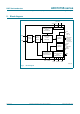
ADC1015S series NXP Semiconductors Single 10-bit ADC; input buffer; CMOS or LVDS DDR digital outputs package ESD parasitics switch INP Ron = 15 Ω 8 4 pF sampling capacitor internal clock INPUT BUFFER switch INM Ron = 15 Ω 7 4 pF sampling capacitor internal clock 005aaa107 Fig 14.
ADC1015S series NXP Semiconductors Single 10-bit ADC; input buffer; CMOS or LVDS DDR digital outputs The configuration shown in Figure 16 is recommended for high frequency applications. In both cases, the choice of transformer is a compromise between cost and performance. ADT1-1WT Analog input 100 nF ADT1-1WT 100 nF INP 50 Ω 100 Ω 50 Ω 100 nF INM VCM 100 nF 100 nF 100 nF 005aaa109 Fig 16. Dual transformer configuration suitable for high intermediate frequency application 11.
ADC1015S series NXP Semiconductors Single 10-bit ADC; input buffer; CMOS or LVDS DDR digital outputs REFAT/ REFBT REFERENCE AMP REFAB/ REFBB VREF EXT_ref EXT_ref BUFFER BANDGAP REFERENCE ADC CORE SENSE SELECTION LOGIC 005aaa164 Fig 17. Reference equivalent schematic If bit INTREF_EN is set to logic 0, the reference voltage is determined either internally or externally as detailed in Table 11. Table 11.
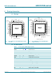
ADC1015S series NXP Semiconductors Single 10-bit ADC; input buffer; CMOS or LVDS DDR digital outputs VREF VREF 330 pF 330 pF REFERENCE EQUIVALENT SCHEMATIC REFERENCE EQUIVALENT SCHEMATIC SENSE SENSE 005aaa117 005aaa116 Fig 18. Internal reference, 2 V (p-p) full-scale Fig 19. Internal reference, 1 V (p-p) full-scale VREF V 0.1 μF VREF 330 pF REFERENCE EQUIVALENT SCHEMATIC REFERENCE EQUIVALENT SCHEMATIC SENSE VDDA SENSE 005aaa119 005aaa118 Fig 20.
ADC1015S series NXP Semiconductors Single 10-bit ADC; input buffer; CMOS or LVDS DDR digital outputs 11.4 Clock input 11.4.1 Drive modes The ADC1015S can be driven differentially (LVPECL). It can also be driven by a single-ended Low Voltage Complementary Metal Oxide Semiconductor (LVCMOS) signal connected to pin CLKP (pin CLKM should be connected to ground via a capacitor) or CLKM (pin CLKP should be connected to ground via a capacitor).
ADC1015S series NXP Semiconductors Single 10-bit ADC; input buffer; CMOS or LVDS DDR digital outputs 11.4.2 Equivalent input circuit The equivalent circuit of the input clock buffer is shown in Figure 24. The common-mode voltage of the differential input stage is set via internal 5 k resistors. Package ESD Parasitics CLKP Vcm(clk) SE_SEL SE_SEL 5 kΩ 5 kΩ CLKM 005aaa056 Vcm(clk) = common-mode voltage of the differential input stage. Fig 24.
ADC1015S series NXP Semiconductors Single 10-bit ADC; input buffer; CMOS or LVDS DDR digital outputs 11.5 Digital outputs 11.5.1 Digital output buffers: CMOS mode The digital output buffers can be configured as CMOS by setting bit LVDS_CMOS to logic 0 (see Table 23). Each digital output has a dedicated output buffer. The equivalent circuit of the CMOS digital output buffer is shown in Figure 25. The buffer is powered by a separate OGND/VDDO to ensure 1.8 V to 3.
ADC1015S series NXP Semiconductors Single 10-bit ADC; input buffer; CMOS or LVDS DDR digital outputs 11.5.2 Digital output buffers: LVDS DDR mode The digital output buffers can be configured as LVDS DDR by setting bit LVDS_CMOS to logic 1 (see Table 23). VCCO 3.5 mA typ − + DnP/Dn + 1P 100 Ω RECEIVER DnM/Dn + 1M − + OGND 005aaa058 Fig 26.
ADC1015S series NXP Semiconductors Single 10-bit ADC; input buffer; CMOS or LVDS DDR digital outputs Table 13. LVDS DDR output register 2 …continued LVDS_INT_TER[2:0] Resistor value () 101 100 110 81 111 60 11.5.3 DAta Valid (DAV) output clock A data valid output clock signal (DAV) is provided that can be used to capture the data delivered by the ADC1015S. Detailed timing diagrams for CMOS and LVDS DDR modes are provided in Figure 4 and Figure 5 respectively. 11.5.
ADC1015S series NXP Semiconductors Single 10-bit ADC; input buffer; CMOS or LVDS DDR digital outputs 11.5.7 Output codes versus input voltage Table 15. Output codes VINP VINM Offset binary Two’s complement OTR pin < 1 00 0000 0000 10 0000 0000 1 1.0000000 00 0000 0000 10 0000 0000 0 0.9980469 00 0000 0001 10 0000 0001 0 0.9960938 00 0000 0010 10 0000 0010 0 0.9941406 00 0000 0011 10 0000 0011 0 0.9921875 00 0000 0100 10 0000 0100 0 .... .... .... 0 0.
ADC1015S series NXP Semiconductors Single 10-bit ADC; input buffer; CMOS or LVDS DDR digital outputs Table 17. Number of data bytes to be transferred after the instruction bytes W1 W0 Number of bytes transmitted 0 0 1 byte 0 1 2 bytes 1 0 3 bytes 1 1 4 bytes or more Bits A12 to A0 indicate the address of the register being accessed. In the case of a multiple byte transfer, this address is the first register to be accessed. An address counter is increased to access subsequent addresses.
ADC1015S series NXP Semiconductors Single 10-bit ADC; input buffer; CMOS or LVDS DDR digital outputs CS SCLK (Data format) SDIO (CMOS LVDS DDR) Offset binary, LVDS DDR default mode at start-up 005aaa063 Fig 29. Default mode at start-up: SCLK LOW = offset binary; SDIO HIGH = LVDS DDR CS SCLK (Data format) SDIO (CMOS LVDS DDR) two's complement, CMOS default mode at start-up 005aaa064 Fig 30.
xxxxxxxxxxxxxxxxxxxxx xxxxxxxxxxxxxxxxxxxxxxxxxx xxxxxxx x x x xxxxxxxxxxxxxxxxxxxxxxxxxxxxxx xxxxxxxxxxxxxxxxxxx xx xx xxxxx xxxxxxxxxxxxxxxxxxxxxxxxxxx xxxxxxxxxxxxxxxxxxx xxxxxx xxxxxxxxxxxxxxxxxxxxxxxxxxxxxxxxxxx xxxxxxxxxxxx x x xxxxxxxxxxxxxxxxxxxxx xxxxxxxxxxxxxxxxxxxxxxxxxxxxxx xxxxx xxxxxxxxxxxxxxxxxxxxxxxxxxxxxxxxxxxxxxxxxxxxxxxxxx xxxxxxxx xxxxxxxxxxxxxxxxxxxxxxxxx xxxxxxxxxxxxxxxxxxxx xxx Table 18. NXP Semiconductors ADC1015S_SER Product data sheet 11.6.
ADC1015S series NXP Semiconductors Single 10-bit ADC; input buffer; CMOS or LVDS DDR digital outputs Table 19. Reset and operating mode control register (address 0005h) bit description Default values are highlighted.
ADC1015S series NXP Semiconductors Single 10-bit ADC; input buffer; CMOS or LVDS DDR digital outputs Table 21. Internal reference control register (address 0008h) bit description Default values are highlighted. Bit Symbol 7 to 4 - 3 INTREF_EN 2 to 0 INTREF[2:0] Access Value Description 0000 not used R/W programmable internal reference enable 0 disable 1 active R/W programmable internal reference 000 0 dB (FS = 2 V) 001 1 dB (FS = 1.78 V) 010 2 dB (FS = 1.
ADC1015S series NXP Semiconductors Single 10-bit ADC; input buffer; CMOS or LVDS DDR digital outputs Table 23. Output data standard control register (address 0011h) bit description …continued Default values are highlighted. Bit Symbol Access 1 to 0 DATA_FORMAT[1:0] R/W Value Description output data format 00 offset binary 01 two’s complement 10 gray code 11 offset binary Table 24. Output clock register (address 0012h) bit description Default values are highlighted.
ADC1015S series NXP Semiconductors Single 10-bit ADC; input buffer; CMOS or LVDS DDR digital outputs Table 26. Test pattern register 1 (address 0014h) bit description …continued Default values are highlighted. Bit Symbol Access 2 to 0 TESTPAT_SEL[2:0] R/W Value Description digital test pattern select 000 off 001 mid scale 010 FS 011 +FS 100 toggle ‘1111..1111’/’0000..0000’ 101 custom test pattern 110 ‘1010..1010.’ 111 ‘010..1010’ Table 27.
ADC1015S series NXP Semiconductors Single 10-bit ADC; input buffer; CMOS or LVDS DDR digital outputs Table 30. CMOS output register (address 0020h) bit description Default values are highlighted. Bit Symbol 7 to 4 - 3 to 2 DAV_DRV[1:0] 1 to 0 DATA_DRV[1:0] Access Value Description 0000 not used R/W drive strength for DAV CMOS output buffer 00 low 01 medium 10 high 11 very high R/W drive strength for DATA CMOS output buffer 00 low 01 medium 10 high 11 very high Table 31.
ADC1015S series NXP Semiconductors Single 10-bit ADC; input buffer; CMOS or LVDS DDR digital outputs Table 32. LVDS DDR output register 2 (address 0022h) bit description Default values are highlighted.
ADC1015S series NXP Semiconductors Single 10-bit ADC; input buffer; CMOS or LVDS DDR digital outputs 12. Package outline HVQFN40: plastic thermal enhanced very thin quad flat package; no leads; 40 terminals; body 6 x 6 x 0.85 mm A B D SOT618-6 terminal 1 index area E A A1 c detail X e1 1/2 e e 11 20 C C A B C v w b y1 C y L 21 10 e e2 Eh 1/2 e 1 terminal 1 index area 30 40 31 X Dh 0 2.5 Dimensions Unit mm 5 mm scale A(1) A1 b max 1.00 0.05 0.30 nom 0.85 0.02 0.21 min 0.
ADC1015S series NXP Semiconductors Single 10-bit ADC; input buffer; CMOS or LVDS DDR digital outputs 13. Revision history Table 33. Revision history Document ID Release date Data sheet status Change notice Supersedes ADC1015S_SER v.2 20101220 Product data sheet - ADC1015S_SER v.1 Modifications: ADC1015S_SER v.1 ADC1015S_SER Product data sheet • • • Data sheet status changed from Preliminary to Product. Text and drawings updated throughout entire data sheet. Section 10.
ADC1015S series NXP Semiconductors Single 10-bit ADC; input buffer; CMOS or LVDS DDR digital outputs 14. Legal information 14.1 Data sheet status Document status[1][2] Product status[3] Definition Objective [short] data sheet Development This document contains data from the objective specification for product development. Preliminary [short] data sheet Qualification This document contains data from the preliminary specification.
ADC1015S series NXP Semiconductors Single 10-bit ADC; input buffer; CMOS or LVDS DDR digital outputs Non-automotive qualified products — Unless this data sheet expressly states that this specific NXP Semiconductors product is automotive qualified, the product is not suitable for automotive use. It is neither qualified nor tested in accordance with automotive testing or application requirements.
ADC1015S series NXP Semiconductors Single 10-bit ADC; input buffer; CMOS or LVDS DDR digital outputs 16. Contents 1 2 3 4 5 6 6.1 6.2 7 8 9 10 10.1 10.2 10.3 10.4 11 11.1 11.1.1 11.1.2 11.1.3 11.1.4 11.2 11.2.1 11.2.2 11.3 11.3.1 11.3.2 11.3.3 11.3.4 11.4 11.4.1 11.4.2 11.4.3 11.4.4 11.5 11.5.1 11.5.2 11.5.3 11.5.4 11.5.5 11.5.6 11.5.7 11.6 11.6.1 11.6.2 General description . . . . . . . . . . . . . . . . . . . . . . 1 Features and benefits . . . . . . . . . . . . . . . . . . . . 1 Applications . . . .