
Datasheet

ADC1015S_SER All information provided in this document is subject to legal disclaimers. © NXP B.V. 2010. All rights reserved.
Product data sheet Rev. 2 — 20 December 2010 20 of 42
NXP Semiconductors
ADC1015S series
Single 10-bit ADC; input buffer; CMOS or LVDS DDR digital outputs
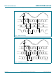
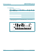
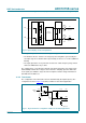
The configuration shown in Figure 16 is recommended for high frequency applications. In
both cases, the choice of transformer is a compromise between cost and performance.
11.3 System reference and power management
11.3.1 Internal/external references
The ADC1015S has a stable and accurate built-in internal reference voltage to adjust the
ADC full-scale. This reference voltage can be set internally via SPI or with pins VREF and
SENSE (programmable in 1 dB steps between 0 dB and 6 dB via control bits
INTREF[2:0] when bit INTREF_EN = logic 1; see Table 21
). See Figure 18 to Figure 21.
The equivalent reference circuit is shown in Figure 17
. External reference is also possible
by providing a voltage on pin VREF as described in Figure 20
.
Fig 16. Dual transformer configuration suitable for high intermediate frequency
application
005aaa109
100 nF
100 nF
100 nF
INP
INM
100 Ω
50 Ω
50 Ω
ADT1-1WTADT1-1WT
Analog
input
100 nF
100 nF
VCM
100 nF