
Datasheet

NXP Semiconductors
ADC1015S series
Single 10-bit ADC; input buffer; CMOS or LVDS DDR digital outputs
© NXP B.V. 2010. All rights reserved.
For more information, please visit: http://www.nxp.com
For sales office addresses, please send an email to: salesaddresses@nxp.com
Date of release: 20 December 2010
Document identifier: ADC1015S_SER
Please be aware that important notices concerning this document and the product(s)
described herein, have been included in section ‘Legal information’.
16. Contents
1 General description. . . . . . . . . . . . . . . . . . . . . . 1
2 Features and benefits . . . . . . . . . . . . . . . . . . . . 1
3 Applications . . . . . . . . . . . . . . . . . . . . . . . . . . . . 2
4 Ordering information. . . . . . . . . . . . . . . . . . . . . 2
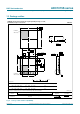
5 Block diagram . . . . . . . . . . . . . . . . . . . . . . . . . . 3
6 Pinning information. . . . . . . . . . . . . . . . . . . . . . 4
6.1 Pinning . . . . . . . . . . . . . . . . . . . . . . . . . . . . . . . 4
6.2 Pin description . . . . . . . . . . . . . . . . . . . . . . . . . 4
7 Limiting values. . . . . . . . . . . . . . . . . . . . . . . . . . 6
8 Thermal characteristics . . . . . . . . . . . . . . . . . . 6
9 Static characteristics. . . . . . . . . . . . . . . . . . . . . 7
10 Dynamic characteristics . . . . . . . . . . . . . . . . . 10
10.1 Dynamic characteristics . . . . . . . . . . . . . . . . . 10
10.2 Clock and digital output timing . . . . . . . . . . . . 12
10.3 SPI timings . . . . . . . . . . . . . . . . . . . . . . . . . . . 15
10.4 Typical characteristics . . . . . . . . . . . . . . . . . . 16
11 Application information. . . . . . . . . . . . . . . . . . 17
11.1 Device control. . . . . . . . . . . . . . . . . . . . . . . . . 17
11.1.1 SPI and Pin control modes . . . . . . . . . . . . . . . 17
11.1.2 Operating mode selection. . . . . . . . . . . . . . . . 18
11.1.3 Selecting the output data standard. . . . . . . . . 18
11.1.4 Selecting the output data format. . . . . . . . . . . 18
11.2 Analog inputs . . . . . . . . . . . . . . . . . . . . . . . . . 18
11.2.1 Input stage . . . . . . . . . . . . . . . . . . . . . . . . . . . 18
11.2.2 Transformer . . . . . . . . . . . . . . . . . . . . . . . . . . 19
11.3 System reference and power management . . 20
11.3.1 Internal/external references . . . . . . . . . . . . . . 20
11.3.2 Programmable full-scale. . . . . . . . . . . . . . . . . 22
11.3.3 Common-mode output voltage (V
O(cm)
) . . . . . 22
11.3.4 Biasing . . . . . . . . . . . . . . . . . . . . . . . . . . . . . . 22
11.4 Clock input . . . . . . . . . . . . . . . . . . . . . . . . . . . 23
11.4.1 Drive modes . . . . . . . . . . . . . . . . . . . . . . . . . 23
11.4.2 Equivalent input circuit . . . . . . . . . . . . . . . . . . 24
11.4.3 Duty cycle stabilizer . . . . . . . . . . . . . . . . . . . . 24
11.4.4 Clock input divider . . . . . . . . . . . . . . . . . . . . . 24
11.5 Digital outputs. . . . . . . . . . . . . . . . . . . . . . . . . 25
11.5.1 Digital output buffers: CMOS mode . . . . . . . . 25
11.5.2 Digital output buffers: LVDS DDR mode. . . . . 26
11.5.3 DAta Valid (DAV) output clock . . . . . . . . . . . . 27
11.5.4 Out-of-Range (OTR). . . . . . . . . . . . . . . . . . . . 27
11.5.5 Digital offset . . . . . . . . . . . . . . . . . . . . . . . . . . 27
11.5.6 Test patterns . . . . . . . . . . . . . . . . . . . . . . . . . . 27
11.5.7 Output codes versus input voltage . . . . . . . . . 28
11.6 Serial peripheral interface. . . . . . . . . . . . . . . . 28
11.6.1 Register description . . . . . . . . . . . . . . . . . . . . 28
11.6.2 Default modes at start-up . . . . . . . . . . . . . . . . 29
11.6.3 Register allocation map . . . . . . . . . . . . . . . . . 31
12 Package outline. . . . . . . . . . . . . . . . . . . . . . . . 38
13 Revision history . . . . . . . . . . . . . . . . . . . . . . . 39
14 Legal information . . . . . . . . . . . . . . . . . . . . . . 40
14.1 Data sheet status. . . . . . . . . . . . . . . . . . . . . . 40
14.2 Definitions . . . . . . . . . . . . . . . . . . . . . . . . . . . 40
14.3 Disclaimers . . . . . . . . . . . . . . . . . . . . . . . . . . 40
14.4 Trademarks . . . . . . . . . . . . . . . . . . . . . . . . . . 41
15 Contact information . . . . . . . . . . . . . . . . . . . . 41
16 Contents. . . . . . . . . . . . . . . . . . . . . . . . . . . . . . 42