
Datasheet


ADC1115S125 All information provided in this document is subject to legal disclaimers. © NXP B.V. 2010. All rights reserved.
Product data sheet Rev. 2 — 17 December 2010 13 of 38
NXP Semiconductors
ADC1115S125
11-bit, 125 Msps ADC; input buffer; CMOS or LVDS DDR digital outputs
11. Application information
11.1 Device control
The ADC1115S125 can be controlled via the Serial Peripheral Interface (SPI control
mode) or directly via the I/O pins (Pin control mode).
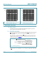
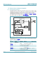
11.1.1 SPI and Pin control modes
The device enters Pin control mode at power-up, and remains in this mode as long as pin
CS
is held HIGH. In Pin control mode, the SPI pins SDIO, CS and SCLK are used as
static control pins.
SPI control mode is enabled by forcing pin CS
LOW. Once SPI control mode has been
enabled, the device remains in this mode. The transition from Pin control mode to SPI
control mode is illustrated in Figure 13
.
When the device enters SPI control mode, the output data standard and data format are
determined by the level on pin SDIO as soon as a transition is triggered by a falling edge
on CS
.
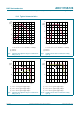
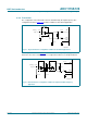
Fig 11. Spurious-free dynamic range as a function of
common-mode input voltage (V
i(cm)
)
Fig 12. Signal-to-noise ratio as a function of
common-mode input voltage (V
i(cm)
)
V
I(cm)
(V)
3.52.50.5 3.02.01.00 1.5
001aam659
78
74
86
82
90
SFDR
(dBc)
70
V
I(cm)
(V)
3.52.50.5 3.02.01.00 1.5
001aam660
69
67
73
71
75
SNR
(dBFS)
65
Fig 13. Control mode selection
R/W
SPI control mode
Pin control mode
Data format
offset binary
Data format
two's complement
LVDS DDR
SDIO/ODS
SCLK/DFS
W1 W0 A12
005aaa03
9
CMOS
CS