
Datasheet


ADC1415S_SER All information provided in this document is subject to legal disclaimers. © NXP B.V. 2010. All rights reserved.
Product data sheet Rev. 4 — 17 December 2010 21 of 42
NXP Semiconductors
ADC1415S series
Single 14-bit ADC; input buffer; CMOS or LVDS DDR digital outputs
11.3 System reference and power management
11.3.1 Internal/external references
The ADC1415S has a stable and accurate built-in internal reference voltage to adjust the
ADC full-scale. This reference voltage can be set internally via SPI or with pins VREF and
SENSE (programmable in 1 dB steps between 0 dB and −6 dB via control bits
INTREF[2:0] when bit INTREF_EN = logic 1; see Table 21
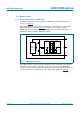
) See Figure 18 to Figure 21.
The equivalent reference circuit is shown in Figure 17
. External reference is also possible
by providing a voltage on pin VREF as described in Figure 20
.
If bit INTREF_EN is set to logic 0, the reference voltage is determined either internally or
externally as detailed in Table 11
.
[1] The voltage on pin VREF is doubled internally to generate the internal reference voltage.
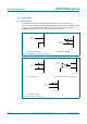
Fig 17. Reference equivalent schematic
Table 11. Reference selection
Selection SPI bit
INTREF_EN
SENSE pin VREF pin Full-scale (p-p)
internal
(Figure 18
)
0 AGND 330 pF capacitor to AGND 2 V
internal
(Figure 19
)
0 pin VREF connected to pin SENSE and
via a 330 pF capacitor to AGND
1 V
external
(Figure 20
)
0V
DDA(3V)
external voltage between
0.5 V and 1 V
[1]
1 V to 2 V
internal via SPI
(Figure 21
)
1 pin VREF connected to pin SENSE and
via 330 pF capacitor to AGND
1 V to 2 V
EXT_ref
EXT_ref
005aaa164
REFAT/
REFBT
REFAB/
REFBB
SENSE
VREF
SELECTION
LOGIC
BANDGAP
REFERENCE
ADC CORE
BUFFER
REFERENCE
AMP