
Datasheet


ADC1415S_SER All information provided in this document is subject to legal disclaimers. © NXP B.V. 2010. All rights reserved.
Product data sheet Rev. 4 — 17 December 2010 33 of 42
NXP Semiconductors
ADC1415S series
Single 14-bit ADC; input buffer; CMOS or LVDS DDR digital outputs
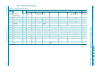
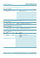
Table 21. Internal reference control register (address 0008h) bit description
Default values are highlighted.
Bit Symbol Access Value Description
7 to 4 - 0000 not used
3 INTREF_EN R/W programmable internal reference enable
0disable
1 active
2 to 0 INTREF[2:0] R/W programmable internal reference
000 0 dB (FS = 2 V)
001 −1dB (FS=1.78V)
010 −2dB (FS=1.59V)
011 −3dB (FS=1.42V)
100 −4dB (FS=1.26V)
101 −5dB (FS=1.12V)
110 −6dB (FS=1V)
111 reserved
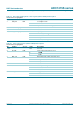
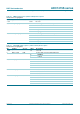
Table 22. Input buffer control register (address 0010h) bit description
Default values are highlighted.
Bit Symbol Access Value Description
7 to 2 - 000000 not used
1 to 0 IB_IBIAS[1:0] R/W input buffer bias current
00 not used
01 medium
10 low
11 high
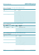
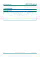
Table 23. Output data standard control register (address 0011h) bit description
Default values are highlighted.
Bit Symbol Access Value Description
7 to 5 - 000 not used
4 LVDS_CMOS R/W output data standard: LVDS DDR or CMOS
0CMOS
1 LVDS DDR
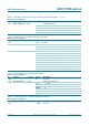
3 OUTBUF R/W output buffers enable
0 output enabled
1 output disabled (high Z)
2 OUTBUS_SWAP R/W output bus swapping
0 no swapping
1 output bus is swapped (MSB becomes LSB and vice versa)