
Datasheet


ADC1415S_SER All information provided in this document is subject to legal disclaimers. © NXP B.V. 2010. All rights reserved.
Product data sheet Rev. 4 — 17 December 2010 34 of 42
NXP Semiconductors
ADC1415S series
Single 14-bit ADC; input buffer; CMOS or LVDS DDR digital outputs
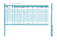
1 to 0 DATA_FORMAT[1:0] R/W output data format
00 offset binary
01 two’s complement
10 gray code
11 offset binary
Table 23. Output data standard control register (address 0011h) bit description
…continued
Default values are highlighted.
Bit Symbol Access Value Description
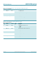
Table 24. Output clock register (address 0012h) bit description
Default values are highlighted.
Bit Symbol Access Value Description
7 to 4 - 0000 not used
3 DAVINV R/W output clock data valid (DAV) polarity
0normal
1inverted
2 to 0 DAVPHASE[2:0] R/W DAV phase select
000 output clock shifted (ahead) by 3 ns
001 output clock shifted (ahead) by 2.5 ns
010 output clock shifted (ahead) by 2 ns
011 output clock shifted (ahead) by 1.5 ns
100 output clock shifted (ahead) by 1 ns
101 output clock shifted (ahead) by 0.5 ns
110 default value as defined in timing section
111 output clock shifted (delayed) by 0.5 ns
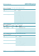
Table 25. Offset register (address 0013h) bit description
Default values are highlighted.
Bit Symbol Access Value Description
7 to 6 - 00 not used
5 to 0 DIG_OFFSET[5:0] R/W digital offset adjustment
011111 +31 LSB
... ...
000000 0
... ...
100000 −32 LSB
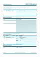
Table 26. Test pattern register 1 (address 0014h) bit description
Default values are highlighted.
Bit Symbol Access Value Description
7 to 3 - 00000 not used