
Datasheet


ADC1415S_SER All information provided in this document is subject to legal disclaimers. © NXP B.V. 2010. All rights reserved.
Product data sheet Rev. 4 — 17 December 2010 37 of 42
NXP Semiconductors
ADC1415S series
Single 14-bit ADC; input buffer; CMOS or LVDS DDR digital outputs
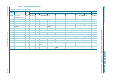
Table 32. LVDS DDR output register 2 (address 0022h) bit description
Default values are highlighted.
Bit Symbol Access Value Description
7 to 4 - 0000 not used
3 BIT/BYTE_WISE R/W DDR mode for LVDS output
0 bit wise (even data bits output on DAV rising edge / odd data
bits output on DAV falling edge)
1 byte wise (MSB data bits output on DAV rising edge / LSB data
bits output on DAV falling edge)
2 to 0 LVDS_INTTER[2:0] R/W internal termination for LVDS buffer (DAV and DATA)
000 no internal termination
001 300 Ω
010 180 Ω
011 110 Ω
100 150 Ω
101 100 Ω
110 81 Ω
111 60 Ω