
Datasheet


BF1118_1118R_1118W_1118WR All information provided in this document is subject to legal disclaimers. © NXP Semiconductors N.V. 2014. All rights reserved.
Product data sheet Rev. 3 — 14 November 2014 3 of 13
NXP Semiconductors
BF1118(R); BF1118W(R)
Silicon RF switches
4. Marking
5. Limiting values
6. Thermal characteristics
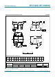
[1] Soldering point of FET gate and diode anode lead.
Table 4. Marking
Type number Marking code
BF1118 VC%
BF1118R VD%
BF1118W VB
BF1118WR VC
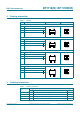
Table 5. Limiting values
In accordance with the Absolute Maximum Rating System (IEC 60134).
Symbol Parameter Conditions Min Max Unit
FET
V
DS
drain-source voltage - 3 V
V
SD
source-drain voltage - 3 V
V
DG
drain-gate voltage - 7 V
V
SG
source-gate voltage - 7 V
I
D
drain current - 10 mA
Diode
V
R
reverse voltage - 35 V
I
F
forward current - 100 mA
FET and diode
T
stg
storage temperature 65 +150 C
T
j
junction temperature - 150 C
Table 6. Thermal characteristics
Symbol Parameter Conditions Typ Unit
R
th(j-sp)
thermal resistance from junction
to solder point
[1]
250 K/W