
Datasheet


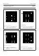


Table Of Contents

2000 Jan 05 3
NXP Semiconductors Product specification
N-channel junction FET BF862
LIMITING VALUES
In accordance with the Absolute Maximum Rating System (IEC 134).
Note
1. Main heat transfer is via the gate lead.
THERMAL CHARACTERISTICS
Note
1. Soldering point of the gate lead.
SYMBOL PARAMETER CONDITIONS MIN. MAX. UNIT
V
DS
drain-source voltage 20 V
V
DG
drain-gate voltage 20 V
V
GS
gate-source voltage 20 V
I
DS
drain-source current 40 mA
I
G
forward gate current 10 mA
P
tot
total power dissipation T
s
90 C; note 1 300 mW
T
stg
storage temperature 65 +150 C
T
j
junction temperature 150 C
SYMBOL PARAMETER CONDITIONS VALUE UNIT
R
th j-s
thermal resistance from junction to soldering
point
note 1 200 K/W
handbook, halfpage
040
T
s
(°C)
P
tot
(mW)
80 160
400
300
100
0
200
120
MCD808
Fig.2 Power derating curve.